A single Operational Floating Current Conveyor (OFCC) based continuous time filter is proposed in this paper. The proposed filter can be configured for low pass, band pass and high pass responses by choosing proper impedances. It shows orthogonal controllability of pole frequency and quality factor. It can provide low pass, high pass and band pass responses by appropriately selecting component values. The verification of the theoretical proposition is done through AC and transient analysis in SPICE. The resilience of the circuit has been tested by the use of Monte Carlo analysis in SPICE.
Continuous Time (CT) filters find wide applications pertaining to electronic systems namely radar, consumer electronics, instrumentation and military ordnance (Su, 2003). The design of CT filters using current mode (CM) building blocks has received considerable interest in past few years due to inherent expedients such as larger bandwidth at higher gains. The Operational Floating Current Conveyor (OFCC) (Ghallab, Badawy, Kaler & Maundy, 2005), a CM active block, is a versatile block in the sense that it has both low and high impedance terminals which facilitates processing of voltage and current signals. Variety of OFCC based circuits such as wheatstone bridge (Ghallab & Badawy, 2006), instrumentation amplifier (Ghallab et al., 2005), readout circuits (Ghallab & Badawy, 2004), rectifier (Pandey, Pandey, Nand& Kumar, 2014), logarithmic amplifier (Pandey, Tripathi, Pandey & Batra, 2014), variable gain amplifier (Hassan & Soliman, 2005), and filters (Ghallab, Badawy, Kaler, Elela & Elsaid, 2002; Ghallab, Elela & Elsaid, 2002; Ghallab, Badawy, Elela & Elsaid 2006; Pandey, Nand & Khan, 2013; Pandey, Nand & Khan, 2014) have been developed in recent past.
This paper addresses the single active block based CT filter which is particularly useful where the power and area constraints are critical. First and second order filter sections are cascaded to obtain higher order filter design to meet desired specifications. In such situation, a multiple active blocks based second order filter will not only lead to a larger silicon area but also higher power consumption as compared to single active block based design.
The objective of the paper is to develop a continuous time filter with moderate component spread, orthogonal tunability, and independent adjustment of angular frequency and gain. The study on OFCC based CT filters (Ghallab et al., 2000; Ghallab et al., 2002; Ghallab et al., 2006; Pandey et al., 2013; Pandey et al., 2014) shows that no single OFCC based filter is available in literature. Therefore, single OFCC based CT filter is proposed in this paper to bridge this gap.
This paper contains five sections including the introductory one. The port relationships of OFCC are given in Section 2 followed by presentation and detailed discussion of the proposed filter. The deviation of the proposed filter behaviour in presence of non-ideality is analysed in Section 3. SPICE simulations in both frequency and time domain are included in Section 4 to verify theoretical proposition. The paper is concluded in Section 5.
The circuit block diagram of OFCC is depicted in Figure 1.
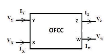
Figure 1. Circuit block of OFCC
It has two inputs (X, Y) and two outputs (W, Z) terminals. The port X has low impedance, and so it is suitable to input current while the port labeled Y presents high input impedance making it ideal for voltage input. The port Z is a high impedance current output. The terminal marked W is the low impedance output voltage.
The transmission properties of the OFCC are given by the matrix in (1):
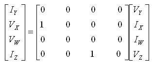
Where Ij and Vj respectively represent current and voltages of jth terminal (j = Y, X, W, Z). Figure 2 depicts proposed filter topology that consists of a single OFCC block along with seven other passive components. The circuit consists of two voltage dividers Z1 and Z4 , cascaded with Z3 and Z5 . But instead as an improvement Z4 is bootstrapped (IEEE 100, 2000) to the output of the amplifier thereby greatly increasing the input impedance of the amplifier and helping control the operating point of the OFCC. Thus, the positive feedback helps improve the Q of the filter and the feedback through Z6 and Z7 , and provide the gain K.
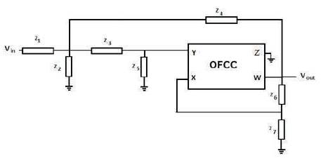
Figure 2. Proposed OFCC Filter
Routine analysis of the circuit of Figure 2 yields in the following transfer function.
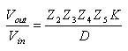
Where


By choosing appropriate impedances in (2), as listed in Table 1, low pass, high pass and band pass frequency responses may be obtained.
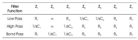
Table 1. Impedance Selection for Different Responses
With the impedance choices list in Table 1, the transfer function for the low pass filter is given as
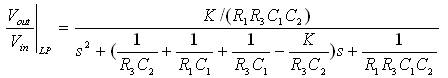
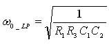
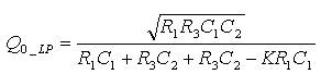
The pole frequency (ω0_ LP ), the quality factor (Q0_LP ), and filter gain (H0_LP ) are computed as:
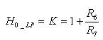
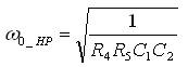
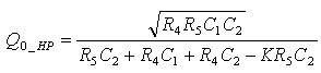
By choosing impedances corresponding to high pass response, the transfer function of (2) becomes,
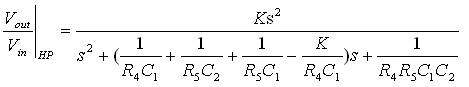
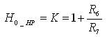
The pole frequency (ω0_HP ), the quality factor (Q0_HP ), and filter gain (H0_HP ) are computed as:
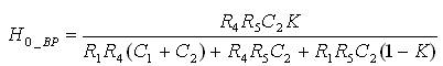
Selecting impedances corresponding to band pass response, the transfer function of (2) modifies to,
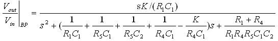
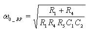
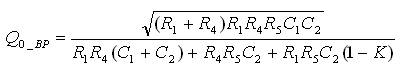
The pole frequency (ω0_BP ), the quality factor (Q0_BP ), and filter gain (H0_BP ) are computed as:
Considering an equicomponent design except for the impedance used to obtain gain i.e. R6 and R7 , filter parameters such as the gain, pole frequency and quality factor of low pass, high pass and band pass responses are placed in Table 2.
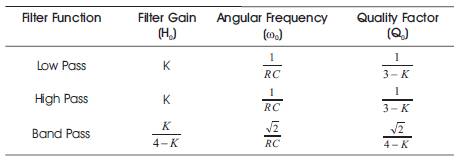
Table 2. Filter Parameters for Equicomponent Design
It is clear from Table 2 that ω0 can be adjusted independent of Q0 . A very high value of Q0 can be obtained by choosing K close to 3 in case of low pass and high pass response. A K close to 4 yields a high Q0 for the band pass response.
The response of the filter often deviates due to the nonideal characteristics of the OFCC. This is due to the parasitic capacitances which causes the gain to be equal to e times its ideal value. Considering the single pole model, the value of ε can generally be approximated as
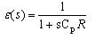
Where Cp is the parasitic capacitance and R is the resistance of the feedback network. This causes the transfer function of the low pass, high pass and band pass topology to modify and become
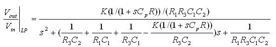
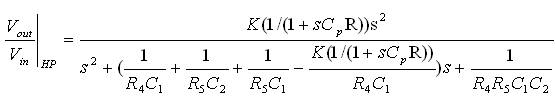
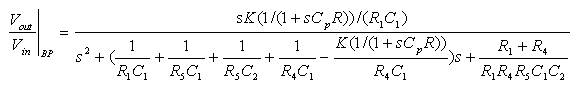
The effect of an additional pole will thus be caused due to the parasitic capacitance which can be ignored by selecting the operating frequency range of this continuous time filter much lower than the parasitic pole frequency.
The OFCC implemented using CMOS (Hassan and Soliman, 2005), as given in Figure 3 is used to verify the operation of the proposed filters. Simulation using SPICE has been done for this purpose using the aspect ratio of various transistors as given in Table 3. Supply voltages (VDD and VSS) are taken as ±1.5V and bias voltages (VB1 and VB2) of ±0.8V are applied.
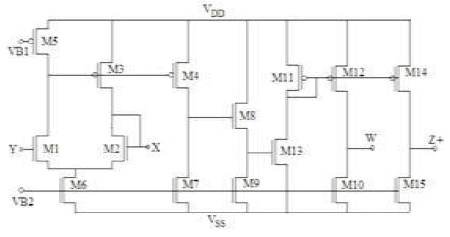
Figure 3. CMOS schematic of OFCC (Hassan and Soliman, 2005)
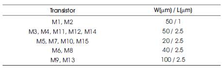
Table 3. Transistors aspect ratios of the circuit shown in Figure 3 (Hassan and Soliman, 2005)
To test the frequency response of the band pass configuration, the filter is designed for center frequency 2.25MHz by taking R1=R4=R5=1KΩ and C1=C2=0.1nF. The values of (R6, R7) are chosen as (1KΩ, 1KΩ), (2KΩ, 1KΩ) and (5.6KΩ, 2KΩ) for Q0=0.71, 1.41 and 7.07 respectively as presented in Figure 4. (a). The frequency response of low pass and high pass configuration for pole frequency of 1.59MHz are presented in Figure 4. (b) where all the resistors and capacitors are taken as 1KΩ and 0.1nF respectively. The low pass and high pass responses with gain 1.5, 2 and 4 while keeping the pole frequency at 1.59MHz are also obtained by choosing (R6, R7) as (1KΩ, 2KΩ), (1KΩ, 1KΩ) and (3KΩ, 1KΩ) respectively. Figure 5 (a) and (b) depict plot to this context. The response to the variation in pole frequency by keeping K constant and taking R1=R4=R5=1KΩ is shown in Figure 6 for band pass filter. The values of (C1, C2) are chosen as (0.1nF, 0.1nF), (0.05nF, 0.05nF) and (0.2nF, 0.2nF) for pole frequency 2.25MHz, 4.5MHz and 1.13MHz respectively.
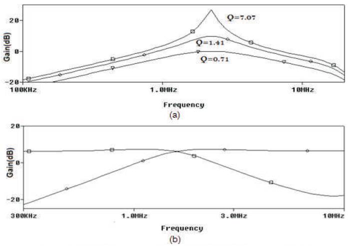
Figure 4 (a) BP Response (Gain) (b) LP & HP Response (Gain)
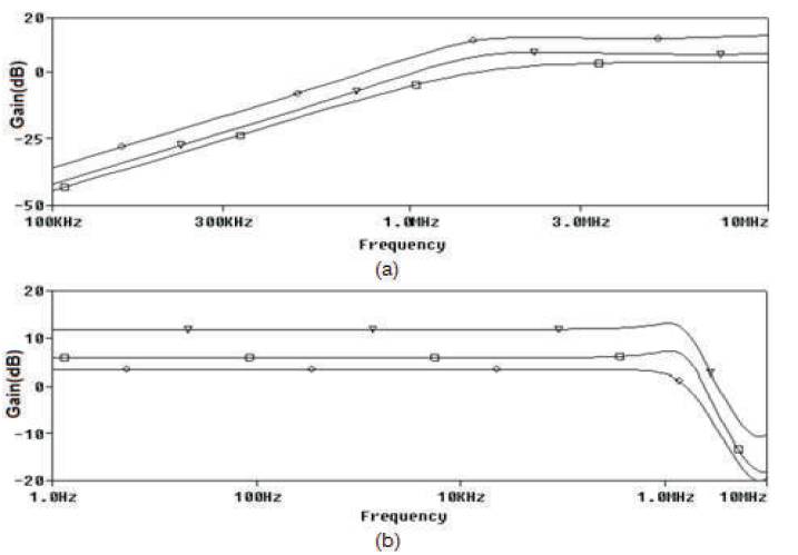
Figure 5 (a) HP Response (constant f0 =1.59 and varying Gain (1.5, 2, 4)), (b) LP Response (constant f0=1.59 and varying Gain (1.5, 2, 4))
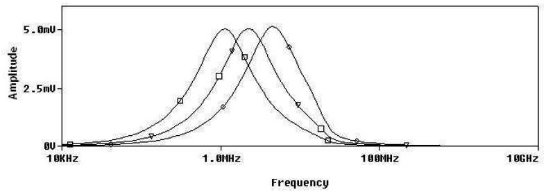
Figure 6. BP Response (f0 =2.25MHz, 4.5MHz and 1.13MHz)
To investigate the time domain behavior of the proposed filter, the band pass topology with f0 =2.25MHz, Q = 0.71 and H = 1 is considered. An input signal of three sinusoids 100 KHz, 1 MHz and 10 MHz is applied. The time domain response and corresponding frequency spectrum is shown in Figure 7 and Figure 8. It is clear that amplitudes of sinusoids having frequency 100 KHz and 10 MHz are significantly deteriorated whereas the signal with 1MHz frequency passes with the minimum deterioration. Another simulation is carried out to check the phase performance of low pass response by applying a sinusoid of 1.59MHz frequency to a filter with f0=1.59MHz. The input and output time domain response are shown in Figure 9. Monte Carlo analysis has been carried out to check the resilience of the circuit. The frequency response of the Monte Carlo analysis with component tolerance of (±5) % is shown in Figure 10.
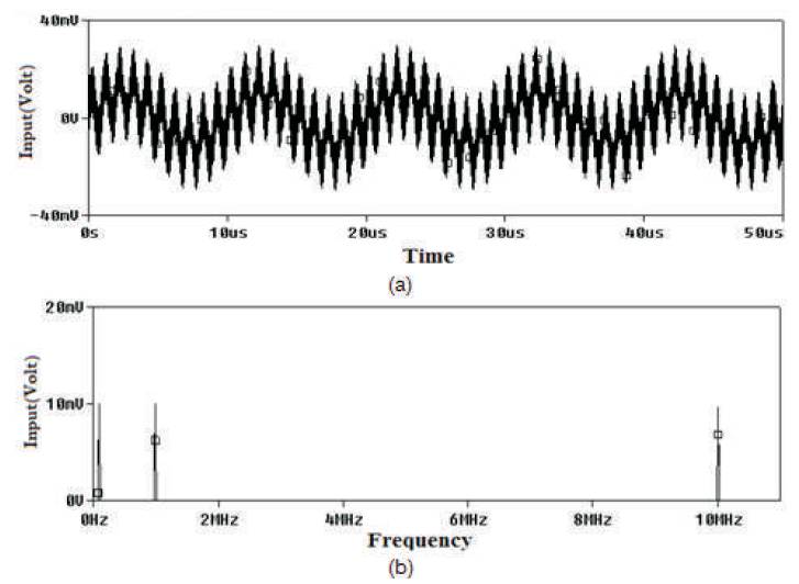
Figure 7 (a) Three source input (b) Three source input (FFT)
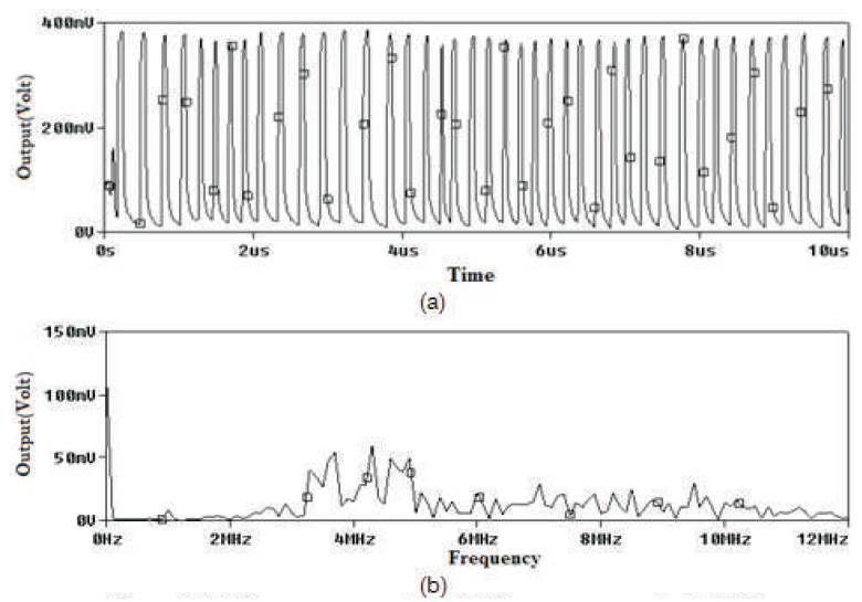
Figure 8 (a) Three source output (b) Three source output (FFT)
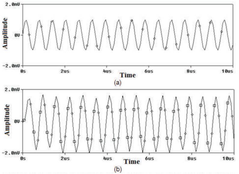
Figure 9 (a) Cut off frequency is equal to source frequency (Input) (b) Cut off frequency is equal to source frequency (Output)
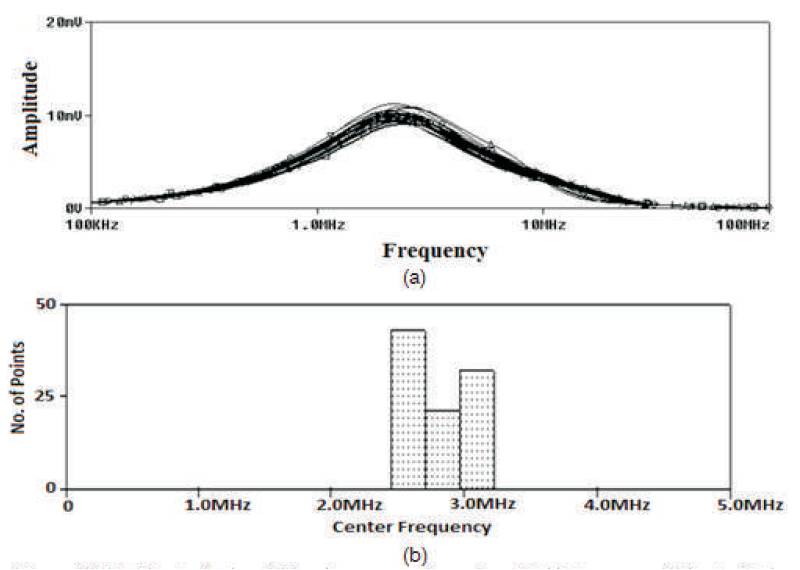
Figure 10 (a) Monte Carlo of Band pass configuration (b) Histogram of Monte Carlo
In this paper, a single OFCC continuous time filter topology is proposed. It can be configured as low pass, band pass and high pass filter upon proper selection of impedance values. The pole frequency, quality factor and bandwidth are controllable using various passive components. The design is simple and the gain can be easily controlled by varying the values of the resistors. The proposed circuit has been tested using SPICE simulations. The results of the time domain, frequency domain and Monte Carlo analysis justify the resilience of the circuit.
The proposed circuit is an ideal replacement in the modern day transceivers. The circuit can work in all three configurations and possesses orthogonal tunability of filter parameters. The filter also provides variation in quality factor and gain, independent of the center frequency.
Moderate component spread is required to achieve high Q factor. The filter possesses high bandwidth and shows immunity to slew related problems. It can thus be used to replace present day filters because of the above mentioned advantages.