In present years, reversible logic has attained importance in many applications in the field of Quantum Computing, Nanotechnology, Low Power CMOS Design, Cryptography, etc. Without reversible logic, it is not possible to realize quantum computing. Code converters are combinational circuits which are used in digital systems designed to enhance the security of data and to decrease the hardware complexity. This paper presents a design for the reversible gray to binary code converter circuit. The main aim in the reversible logic design is to minimize the number of reversible gates used and the garbage output produced. The proposed design is compared to the existing designs in terms of parameters such as reversible gates, constant inputs, garbage outputs, and quantum cost.
In digital circuits, the data are denoted as a group of bits ('0' and '1') known as code. A code is the combination of 0's and 1's to represent the information. A logic circuit which is useful to convert information in one form to another form is known as code converter. In digital domain, different codes are available such as ASCII, Binary Sequence, Gray, Octal, etc. Conversion of code from one format to another format is a prominent process while performing the operations in digital systems such as microprocessor, digital signal processor, etc.
Earlier in 1961, R. Landauer has shown that every bit of information loss will dissipate energy in the form of heat [1]. Later in 1973, C.H. Bennett has proved that the energy loss in a circuit can be ideally decreased to zero, by using reversible logic gates for the designing of circuits [2].
A reversible gate is a m-inputs and m-outputs logic circuit in which there is a one to one mapping between input vectors and output vectors. Some important reversible gates are shown in Table 1. Few main parameters which play a major role in reversible circuit design are listed below.
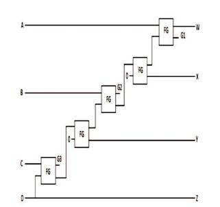
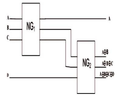
Till today only few researchers have worked in the area of designing a gray to binary code converter using reversible logic approach. In 2013, M. Saravanan and M. Suresh Manic presented the reversible gray to binary code converter using five Feynman gates [3] shown in Figure 1 [6]. This design requires two constant inputs and produce three garbage outputs. Quantum cost of this design was evaluated as five. Later in 2014, Kotaiah Kamani et al. proposed new reversible logic gates named as NG1 and NG2 of 3x3 size. They have designed a gray to binary code converter with reversible approach using a combination of NG1 and NG2. This circuit has used two reversible logic gates as shown in Figure 2 and the quantum cost of this circuit has not reported in the literature [7].

Figure 1. Existing Design 1

Figure 2. Existing Design 2
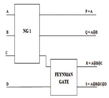
This paper proposes a design for gray to binary code converter circuit using reversible logic gates as shown in Figure 3. The proposed design uses two reversible gates. The reversible gates used in the design are NG1 and Feynman. This design does not need any constant inputs and generates no garbage outputs.

Figure 3. The Proposed Design
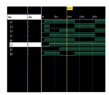
The proposed reversible gray to binary code converter circuit was logically verified through simulations as shown in Figure 4. The Verilog HDL is used to code the proposed reversible design, the test benches are created and simulations are made to verify the correctness of the proposed design.

Figure 4. Simulation Result of the Proposed Design
This paper shows the gray to binary code converter circuit implemented using NG1 and Feynman reversible logic gates. The logical correctness of the proposed design were verified using Verilog Hardware description language in Xilinx 14.1. The parameters of the proposed design were evaluated and compared with the existing designs in terms of number of reversible gates used, constant inputs applied, garbage outputs generated and quantum cost of the reversible digital circuit shown in Table 2. The proposed design of reversible gray to binary code converters will find applications in quantum computing, nanotechnology, etc.

Table 2. Comparison Table of the Proposed Design with the Existing Designs