 |
i-manager's Journal on Instrumentation and Control Engineering |
View PDF |
|||
| Volume :4 | No :1 | Issue :-2016 | Pages :1-9 | ||
Today the expanding use of power inverters in the power electronics industry has increased the importance of applied inverter choosing with respect to the harmonic content and efficiency. Especially, harmonics are playing the most important role because sensitive electronic devices can be operated only with the clean power generated inverters. In this paper, comparative analysis of single phase power inverters regarding their output waveforms was performed. Square wave, modified square wave and true sine wave inverter circuits with 500W rated power were designed and analyzed using Proteus Professional spice program. This comparison was fulfilled in accordance with the circuit configuration, THD (Total Harmonic Distortion) and output efficiency. After simulation results, these inverter circuits were realized on PCB (Printed Circuit Board). The efficiency of the inverters was calculated using Extech true RMS (Root Mean Square) digital multimeter and THD values were measured using Fluke 435 Power Analyzer device. According to the experimental results, the finished true sine wave inverter circuit with about 7% THD and an efficiency of 80% has the most ideal output signal compared to the modified and square wave inverter circuits. To get a resembled sine wave, a low pass filter was designed and applied at the output of the true sine wave inverter circuit. With the help of this filter circuit, the harmonic content was reduced. Tests on resistive and inductive loads were carried out under laboratory conditions and output signals were observed using Tektronix digital storage oscilloscope. Test results and simulation outcomes were confirmed to each other.
Today with the development of power electronic technology, the inverter has been widely used in many fields around the world. Inverters change DC current to AC current, namely they use DC power supply and creates a AC power supply, usually at a voltage similar to normal mains supply. In other words, it enables to run household appliances from a low voltage DC such as a car battery or a solar power system. An inverter will use different kinds of transistors to continually switch the direction of the voltage to produce a sine wave. This switching or oscillation will happen 50 or 60 times a second, according the required frequency[1-3] .
Generally, there are three types of the output waveforms for the power inverters. According to the output waveforms, inverters can be classified into three groups that are square waveform, modified square waveform and true sine waveform as shown in Figure 1 respectively.
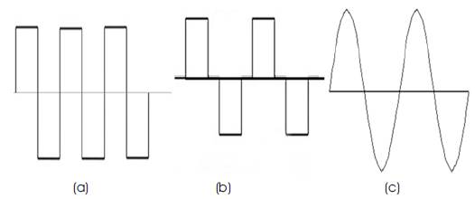
Figure 1. Inverter Output Waveforms (a) Square Waveform, (b) Modified Square Waveform, (c) True Sine Waveform
Today the two dominant commercialized waveforms are modified square wave and true sine wave. Power inverters are widely used for industrial and domestic applications such as renewable energy sources, AC motors, induction heating, and uninterruptible power supplies. They are mainly classified into two types that are single phase and three phases. Each inverter type has controlled turn on and turn off switching devices. Square wave or modified square wave voltages are acceptable only for low and medium power applications, but for high power applications, low distorted sinusoidal waveforms are required. They generally use PWM (Pulse Width Modulation) control signals to get an AC output signal. The output voltage waveforms of the ideal inverters should be sinusoidal, however the waveform of the practical inverters are non-sinusoidal and contains different harmonics. Using high speed power semiconductor devices and different switching techniques, it can reduce the harmonic content at the output voltage [4-9] .
Most of the power inverters draw harmonic current and reactive power and causes power quality problems. Square and modified square wave inverters have more THD at the outputs that causes poor power quality because beside fundamental frequency there are some undesired higher frequencies. But, true sine wave inverters have almost the same signal as of the utility power and as a result they have very low THD and desired power quality. The power quality of an inverter plays an important role for operating sensitive devices. In power electronic, lower THD means pure signal emission without causing interferences such as reduction in peak current, heating in the core or noisy operation for all kinds of electronic devices. With lower THD, an inverter can be used for any devices either for industrial both for domestic appliances [10-12] .
The simplest AC output waveform to generate is a square wave, in which the voltage alternates from positive 220 volts to negative 220 volts, keeping back and forth. This waveform has a lot of THD and results in poor operation of almost any loads. Figure 2 is a single phase power inverter schematic which can generate square wave at the output for 500W. The source of 50 Hz frequency is a 555 timer circuit. The frequency can be set by the resistance values of R2 and capacitor values of C2. As switches two N-type power MOSFETs are applied. One is driven directly from the 555 circuit, the other through a logic inverter with BC547 NPN transistor. Transformer is a main one with two secondary windings 12V and must be designed for the maximum load required. The heat sink of the two power transistors should be in the right size according to the load. The 12V power supply should be sufficiently hard, in the range of about 10 - 15V. The frequency can be set by changing the values of R2 and C2 in the circuit. MOSFETs (Metal-Oxide Semiconductor Field Effect Transistor) can be IRFZ44 for loads up to 500W or IRF3205 above 600W. For output above 600W, multiple transistors should be combined in parallel. This DC/AC power inverter has an output voltage in square waveform and as a result, it has a poor THD at the output voltage.
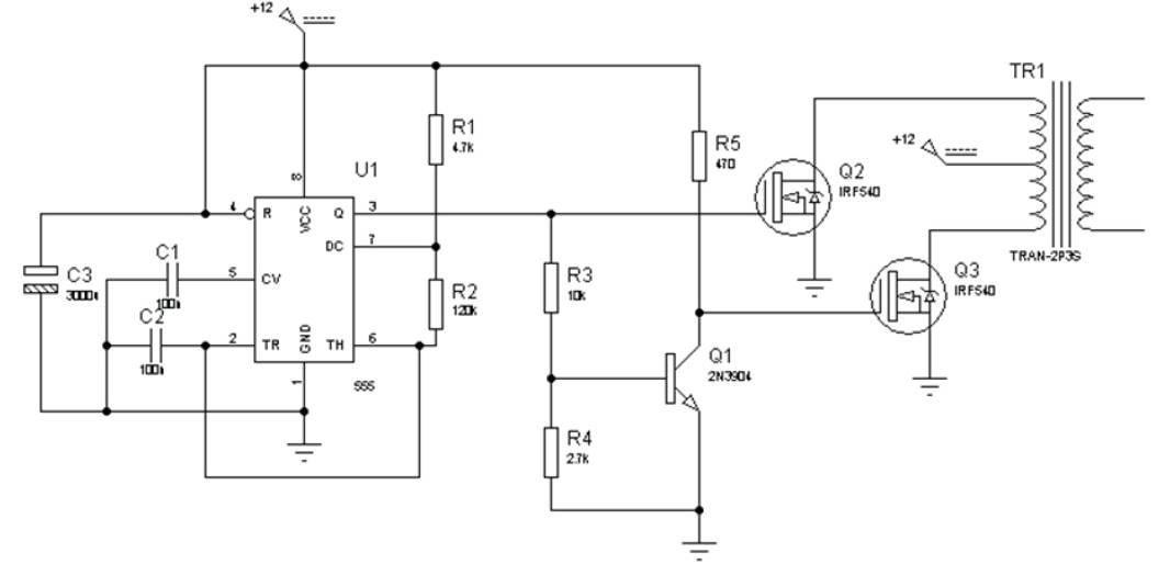
Figure 2. Square Wave Inverter Schematic
Modified Square wave is the term used when the electric current has a constant force, like it has with DC, but switches direction immediately at the same kind of frequency as the normal utility supply. Figure 3 is a single phase modified square wave inverter schematic for 500W. The operating of the circuit is pretty much unique and different from the normal inverters, which include oscillator stage for powering the transistors. The two arms of the inverter circuit operates in a regenerative manner. Due to this, both arms are not able to conduct together at one time. When the upper transistor conducts first, it will be getting their biasing voltage through the lower half winding of the transformer via R7. However, when it saturates and conducts fully, the entire battery voltage is pulled through their collectors to the ground. This gets any voltage through R7 to their base and they immediately stop conducting. This gives an opportunity for the lower transistors to conduct and this cycle repeats. The whole circuit thus starts to oscillate and the output of the circuit is a modified square wave. The base emitter resistors are used to fix a particular threshold for their conduction and they help fixing a base biasing reference level.
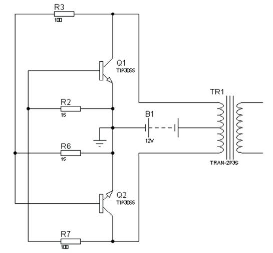
Figure 3. Modified Square Wave Inverter Schematic
True sine wave inverters can operate nearly any load without making problems, and have a better power quality than the utility grid with low THD, since the utility distribution system can be affected negatively by non-linear AC loads resulting in power-quality issues. Figure 4 is a single phase stable and efficient schematic for 500W true sine wave inverter circuit. A simple PIC (Peripheral Interface Controller) micro-controller with its internal clock would produce a stable 50Hz frequency AC output. The PIC16F628A is programmed to produce a logic 5V signal for 5ms at pin 17 then 15ms off. Then, the same process occurs at pin 18, 5ms on then 15ms off. That is, one cycle which is then looped. These two pins are then sent to the gates of the power MOSFET's. These are N-type power MOSFETs that require only 5V to switch ON fully. They have a very low 0.014Ω source to drain resistance, when they are on, which means they can switch high currents without wasting power as heating. This keeps the whole system efficient.
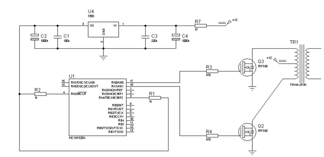
Figure 4. True Sine Wave Inverter Schematic
The MOSFETs could be in parallel pairs for even more power requirements. This circuit can get 220V AC from the 12-0-12 transformer with a 12V standby power sources like a car battery. It has used the low voltage side as the primary, and the high voltage side as the secondary. To get a sinusoidal wave form at the output, it has been used as the passive filter stage consisted of LC components. LC low pass filter only allows low frequency signals from 0Hz to its cut-off frequency to pass while blocking any higher frequencies.
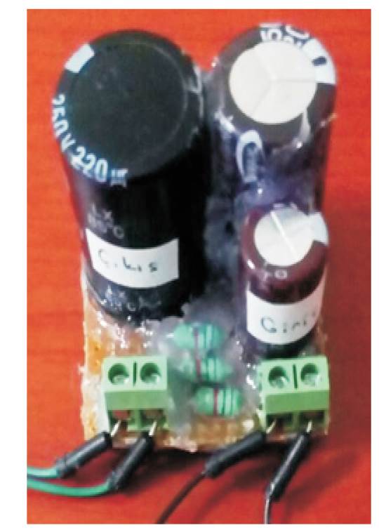
Figure 5. Designed Low Pass Filter
Figure 5 is the designed Low Pass Filter (LPF) circuit for the harmonic elimination. The related equation for resonance frequency (ƒc) is given below:
where,
L stands for inductor and
C for capacitor values:
Assume L = 9µH, and C = 4000µF
 = 500Hz
The filter performance with respect to the output voltage is determined by its resonance frequency. In order to achieve an almost sinusoidal output voltage, the resonance frequency of the filter has to be below the lowest harmonic frequency of the inverter voltage. To avoid additional resonance suppressing control, the resonance frequency has to be above the fundamental frequency of the inverter voltage. The resonance frequency is calculated as about 500Hz, which is greater than the fundamental frequency (50Hz) according to the capacitor (4000μ Farad) and inductor (900μ Henry) values used in the filter stage. While higher harmonics have been eliminated with the help of the low-pass filter circuit, fundamental frequency has passed to the output without filtering[13 -19] .
The simulations have been performed by using Proteus Professional spice program which is wholly unique in offering the ability to simulate the designed circuits. The Proteus Professional spice program combines the schematic capture and ARES PCB layout programs to provide a powerful, integrated and easy to use suite of tools for professional PCB Design.
The comparative analysis is demonstrated via simulations for each inverter circuit using Proteus Professional spice program. After performing of the comparative analysis for the inverters according to the output waveforms, circuit implementations based on the simulation results have been realized. Figures (6 to 9) shows the voltage output waveforms with resistive load and inductive load, oscilloscope observation and harmonic-fourier analysis for square wave inverter circuit respectively.
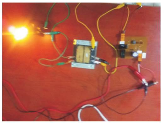
Figure 6. PCB Implementation for Square Wave Inverter
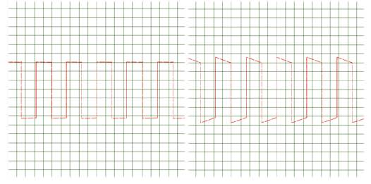
Figure 7. Voltage Output Waveforms with Resistive and Inductive Load for Square Wave Inverter
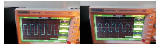
Figure 8. Observation of the Voltage Output Waveforms with Resistive and Inductive Load
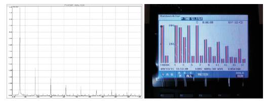
Figure 9. Fourier and Harmonic Analysis of the Voltage Output Waveforms
Figures (10 to 13), represents the voltage output waveforms with resistive load and inductive load, oscilloscope observation and harmonic-fourier analysis for modified square wave inverter circuit respectively.
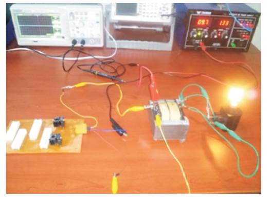
Figure 10. PCB Implementation for Square Wave Inverter
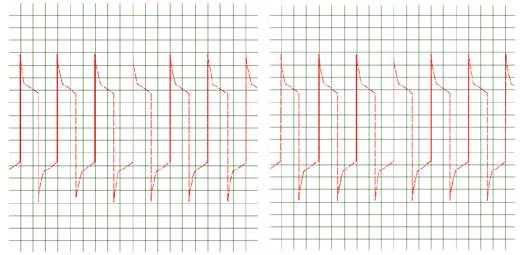
Figure 11. Voltage Output Waveforms with Resistive and Inductive Load for Modified Square Wave Inverter
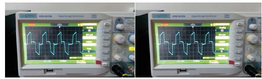
Figure 12. Observation of the Voltage Output Waveforms with Resistive and Inductive Load
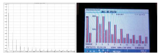
Figure 13. Fourier and Harmonic Analysis of the Voltage Output Waveforms
Figures (14-17) illustrates the voltage output waveforms with resistive load and inductive load, oscilloscope observation and harmonic-fourier analysis for true sine wave inverter circuit respectively.
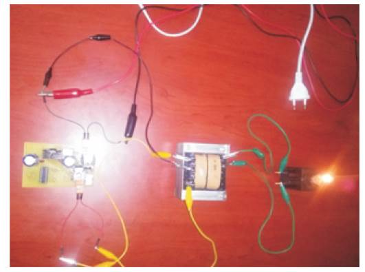
Figure 14. PCB Implementation for True Sine Wave Inverter
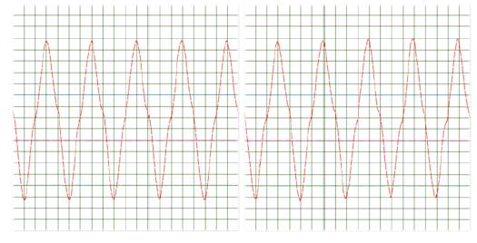
Figure 15. Voltage Output Waveforms with Resistive and Inductive Load for True Sine Wave Inverter
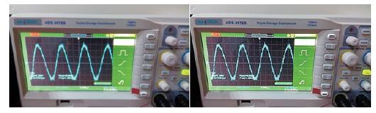
Figure 16. Observation of the Voltage Output Waveforms with Resistive and Inductive Load
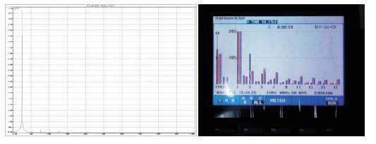
Figure 17. Fourier and Harmonic Analysis of the Voltage Output Waveforms
THD values at the output voltage were calculated by V means of the FLUKE 435 Power Analyzer device for the square wave, modified square wave and true sine wave inverter circuits respectively with the help of the equations. Between the simulation and experimental results, there are only 2% or 3% differences in connection with the used devices and spice program. As mentioned before, THDV, which is the ratio of the RMS (Root Means Square) value of the harmonics (Hn) to the RMS value of the fundamental frequency (H1), can be calculated as follows;

THDV value of the output voltage form is calculated as shown below;

THDV voltage values for the analyzed, square wave inverter with resistive and inductive loads are calculated respectively;


THDV voltage values for the analyzed, modified square wave inverter with resistive and inductive loads are calculated respectively;


THDV voltage values for the analyzed, true sine wave inverter with resistive and inductive loads are calculated respectively;


As it can be seen clearly from the circuit analyses including both simulations and labor experiments, THDV at the output voltages with resistive and inductive loads for the analyzed true sine wave inverter circuit are considerably low while square wave and modified square wave inverter shave higher THDV with resistive and inductive loads that can cause many devices to fail or not working well. True sine wave inverter circuit has at the same time higher efficiency related to the output power in comparison to the other inverter circuits. This is another advantage of the true sine wave inverters on the square and modified square inverters.
In this paper, efficiency comparison has been performed for each designed inverter circuits. For the square wave inverter circuit, the input voltage and current were measured as 10.3V and 1A respectively. The observed output voltage and current under 5W resistive load are about 200V and 24mA respectively. According to the power equation given below, the input and output powers are calculated. The efficiency of the square wave inverter circuit is the ratio of the output power to the input power.
Pin =10.3V×1A=10.3W
Pout =200V×24mA =4.8W
Efficiency= 4.8W/10.3W×100= 46.5%
For the modified square wave inverter circuit, the input voltage and current were measured 7V and 0.8A respectively. The observed output voltage and current under 5W resistive load are circa 200V and 17mA. The input and output powers are calculated as follows.
Pin =7Vz0.8A = 5.6W
Pout =200V×17mA = 3.4W
Efficiency= 3.4W/5.6W× 100= 60.7%
For the true sine wave inverter circuit, the input voltage and current were measured 10.3V and 0.5A respectively. The observed output voltage and current under 5W resistive load are circa 200V and 19mA. The input and output powers are calculated as follows.
Pin =10.3V×0.5A = 5.15W
Pout =200V×19mA = 3.8W
Efficiency= 3.8W/5.05W×100= 75.2%
Besides the efficiency comparison of the analyzed inverters, THD values at the output voltage were calculated V by means of the FLUKE 435 Power Analyzer device for the square wave, modified square wave and true sine wave inverter circuits respectively with the help of the equation shown above. Between the simulation and experimental results there are only 2% or 3% difference in connection with the used devices and simulation program.
In this study, comparative analysis of the single phase power inverters regarding their output waveforms was performed. Square wave, modified square wave and true sine wave inverter circuit's simulations were done by Proteus Professional package program. This comparison was fulfilled with respect to the voltage harmonics and output efficiency. After simulation results, these inverter circuits were realized on PCB and experiments were carried out under laboratory conditions for resistive and inductive loads.
According to the simulation and experimental results, square wave inverter circuit has the more than 55% THDV and circa 45% efficiency. They are used only for some industrial applications, since it is not acceptable to have an output voltage with high THDV. Square wave inverter circuit is the simplest and the least expensive type of inverters, but it produces the lowest quality of power.
Modified square wave inverter circuit has better THDV with about 38% than square wave inverter and better efficiency value of about 60%. For many electronic devices that do not require sensitive power, modified square wave inverters are more cost-effective option. Due to their many advantages, they are widely used in most applications today.
True sine wave inverter circuit has the best THDV circa 10% and highest efficiency about 75%. True sine wave inverters provide clean and stable power like the utility grid and are able to drive all the applications that are sensitive to AC voltage. Their only drawbacks are the high-cost and circuit complexity.
The main objective of this paper is to provide a general notion to the readers who are interested in comparative analysis of the single phase power inverters regarding their output waveforms. The future work includes improving the stability of the system and to study various topologies for achieving higher efficiency.
In this work, single phase inverters according to the output waveforms were compared in details. The advantages and disadvantages were discussed in order to perform which of these inverters should be selected regarding to the requirements. According to the obtained results, square wave and modified square wave inverters are more economical, but true sine wave inverters with very low THD and high efficiency are the best inverters for power industrial applications.
This study was supported by Necmettin Erbakan University Scientific Research Projects Office.
