This paper presents an unique three phase seven level inverter with reduced number of switches. Multilevel Inverters (MLI) are used in high power and high voltage applications as they are capable of producing multiple levels in output voltage with reduced THD. To reduce THD further, the number of levels in the output voltage has to be increased, which is directly associated with the number of switches required. To accomplish this, the conventional MLI experiences complexity in control, number of required DC sources, size, switching losses and cost of overall system increases. The proposed topology overcomes the aforesaid limitations and compared with the conventional MLI in terms of the number of switches, DC sources, capacitors, fundamental voltage, and THD. The performance is analyzed by using a simulation tool.
Based on the circuit configuration, the multilevel inverters are classified as diode clamped, flying capacitor and cascaded [1-3] inverters. Out of which, Cascaded Multilevel Inverter (CMLI) is having more advantages when compared to diode clamped and flying capacitor in terms of the number of switches, control complexity and voltage balancing [3] . Furthermore, clamping diodes and flying capacitors are not required for CMLI With conventional CMLI, the number of levels can be increased by increasing the number of series connected H Bridges. The circuit configuration of three phase CMLI is represented in Figure 1.
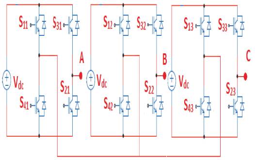
Figure 1. Three Phase CMLI Configuration
This paper presents a novel seven level inverter with reduced number of switches. The numbers of levels are increased by increasing the number of switches instead of adding the H bridge.
The rest of the paper is organized as follows, concept of single phase seven level inverter with reduced number of switches is explained in section 1, the same idea is extended for three phase inverter section 2, different carrier based PWM techniques are discussed in section 3, the simulation results of the proposed and conventional seven level inverters are presented in section 4, finally conclusions are made in the last section .
For reducing the number of components, control complexity, cost and size of multilevel inverter used for high voltage and high power applications of a novel single phase five level inverter is explained [5] . The proposed single phase seven level inverter is represented in Figure 2. The proposed topology is the cascaded linkage of following parts:
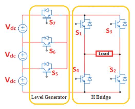
Figure 2. Single Phase Seven Inverter Circuit Configuration
Part I: Level generator which generates the positive stepped waveform across the inverter.
Part II: H Bridge, used for polarity reversal.
The Generalized equation to decide the number of DC sources, and switches required for a proposed MLI is given below:


Where n is the number of levels in output voltage.
The proposed seven level inverter requires three dc sources of equal magnitude and seven switches. Comparison of different components required for conventional and the proposed MLI's is shown in Table 1.
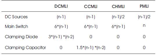
Table 1. Comparison with Conventional MLI
The proposed seven level inverter is capable of producing seven levels ±3Vdc , ±2Vdc , ±Vdc and 0 in the output dc dc dc voltage waveform. The switching sequence t produce these seven levels in the output voltage is shown in Table 2.
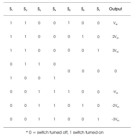
Table 2. Switching Sequence
At any instant only three switches will be conducting. Two switches for polarity reversal and one switch for getting the desired voltage level in the output waveform. Single phase Seven level inverter with nine and ten switches are discussed [6, 7].
The concept of proposed single phase seven level inverter can be easily extended to the three phase seven level inverter. The proposed three phase topology is easy to control as the number of switches conducting at any instant is less when compared with conventional topology. Figure 3, represents the circuit configuration of the proposed three phase seven level inverter.
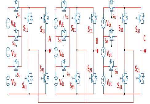
Figure 3. Three Phase Seven Level Inverter
The purpose of PWM is to generate the variable voltage and variable frequency from the fixed DC input. In PWM techniques two signals are used, i.e., carrier and reference signal. When reference is greater than a carrier, ON pulse is generated and OFF pulse is generated when the carrier is greater than the reference [8, 9]. Classification of PWM methods is shown in Figure 4.
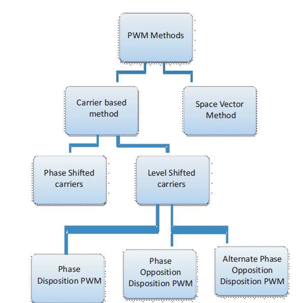
Figure 4. Flow Chart of PWM Methods Classification
With space vector method, the number of switching states is equal to n3 where n represents the number of levels. It is difficult to identify the sectors, sub sector and switching sequence. The phase shifted carriers generates a lot of harmonics in the output voltage. To overcome the intact drawbacks the level shifted carriers are used.
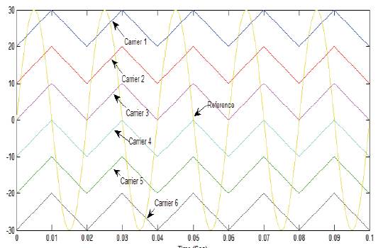
Figure 5. Phase Disposition Carriers
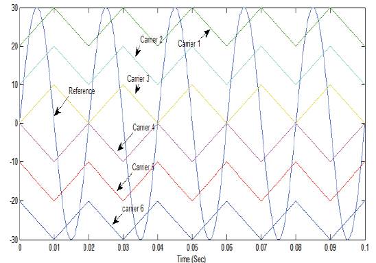
Figure 6. Phase Opposition Disposition Carriers
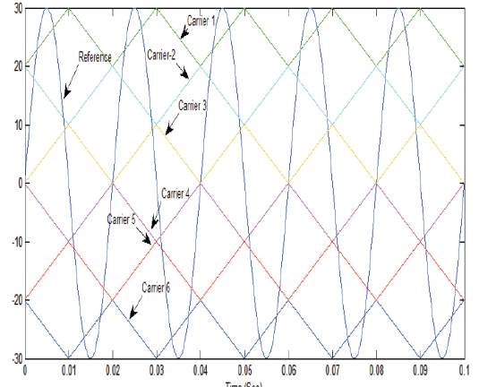
Figure 7. Alternate Phase Opposition Disposition Carriers
Conventional seven level cascaded and proposed seven level inverters are simulated with level shifted carrier PD, POD and APOD. These inverters are simulated with the following parameters,
Input Voltage = 100V,
Switching Frequency = 10000Hz,
Modulation Index = 1
Resistive Load =100 Ω.
Figures 8 to 10 show the simulation results for THD and the output line to line voltage for conventional seven level inverter using PD, POD and APOD PWM techniques respectively.
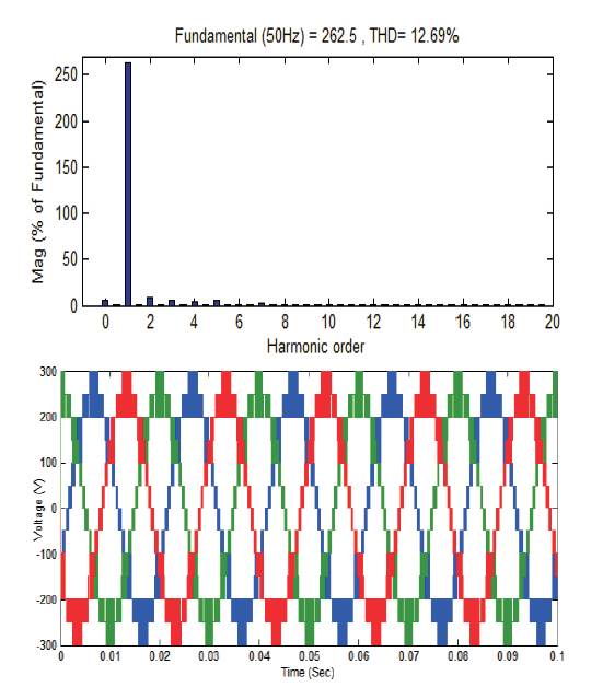
Figure 8. THD and Output Voltage with PD
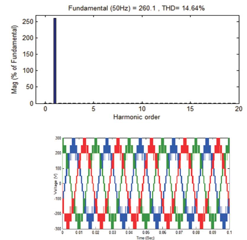
Figure 9. THD and Output Voltage with POD
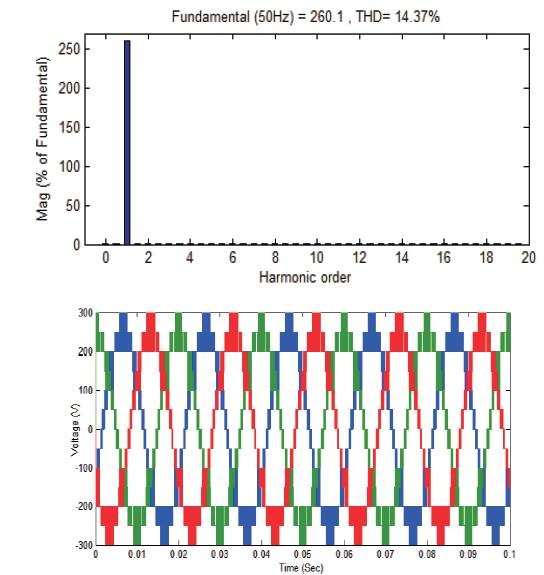
Figure 10. THD and Output Voltage with APOD
Figures 11 to 13 show the THD and the output line to line voltage simulation results for proposed seven level inverter using PD, POD and APOD PWM techniques. The comparison results are shown in Table 3.
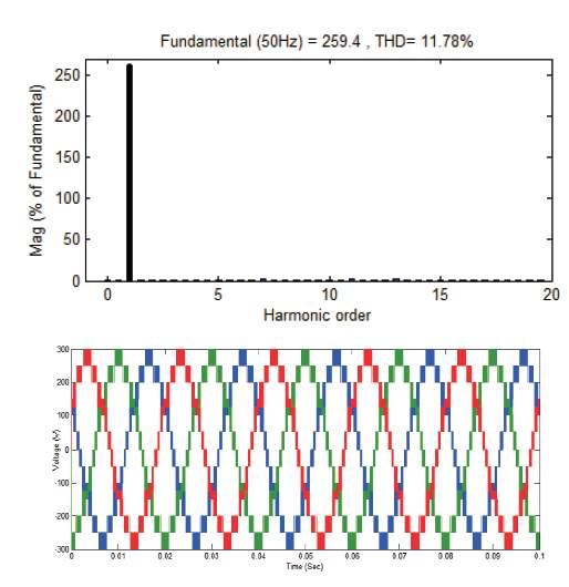
Figure 11. THD and Output Voltage with PD
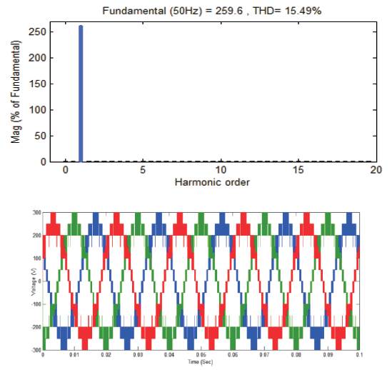
Figure 12. THD and Output Voltage with POD
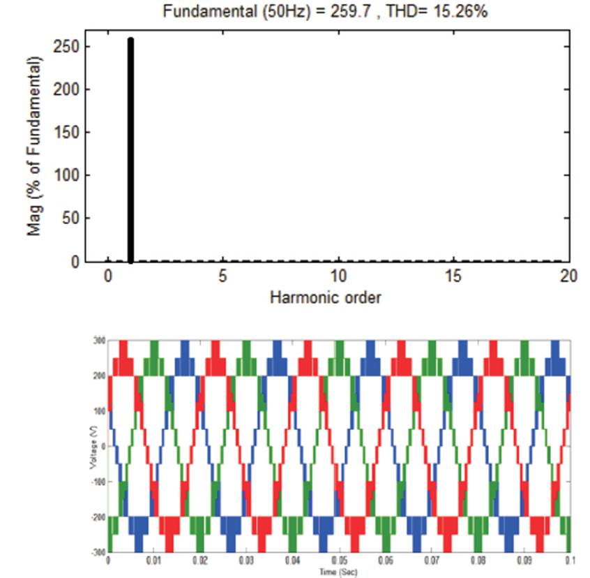
Figure 13. THD and Output Voltage with APOD
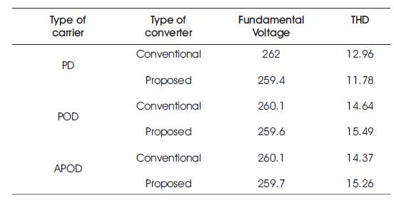
Table 3. Comparison of CMLI's and PMLI
This paper presents a new three phase seven level inverter with reduced number of switches. The proposed inverter is capable of producing the same fundamental voltage and THD as that of conventional seven level cascaded inverter. The proposed circuit reduces the complexity of control, size and cost of the inverter, as the number of components used in this circuit is equal to a number of levels. The same inverter can be extended to n levels with n switches