This paper presents a Second Order Notch/All pass filter based on Operational Transresistance Amplifier (OTRA). It uses two OTRA's and five resistances. To add electronic tunability, the filter uses a capacitor array that can be controlled by switches. The switches are also used to provide inverting and non inverting Notch/All pass as response. This adds flexibility in phase response of all pass filter. The notch/all pass configuration is a modified extension of the Delyiannis-Friend circuit. Through the addition of a second active block which basically acts as a summer for the input voltage and the output of the first OTRA block. The functionality of the proposed filters is verified through SPICE simulations using CMOS based implementation of OTRA. The power supply for the implementation is 1.5V and is based on 0.5 submicron technology.
The OTRA (Cam, Kacar, Cicekoglu, H. Kuntman and A. Kuntman, (2003); Chen, Tsao, Liu and Chiu, (1995); Chien, (2014); Lo, Chien and Chiu, (2009); Mostafa and Soliman, (2006); R. Pandey, N. Pandey, Sriram and Paul, (2012); Salama and Soliman, (1999, 2000)) has emerged as an alternate analog building block since it inherits all the advantages offered by current mode techniques. The OTRA is a high gain current input voltage output device. Due to low impedance input and output terminals, limitations on the response by the time constants of the capacitors are reduced. The device is unaffected by stray capacitances due to virtually grounded inputs (Chien, 2014). Ideally, the transresistance gain of OTRA approaches are infinity and external negative feedback must be used which forces the input currents to be equal.
The continuous time filters are imperative in signal processing applications. The second order filters being basic building block in realisation of higher order filters, are important class of circuit. The notch filters are used to suppress the magnitude of a particular frequency while passing other frequencies un-attenuated. The all pass filter also known as delay equaliser is widely used for linearizing the phase. The literature survey on OTRA based second order notch/all pass filters (Cakir, Cam and Cicekoglu, (2005); Chang, Ko, Guo, Hou and Horng, (2015); Chen, Tsao and Liu, (2001); Chen et al., (1995); Gokcen and Cam, (2009); Gokcen, Kilinc and Cam, (2011); Kilinc and Cam, (2005); Kilinc, Keskin and Cam, (2007); R. Pandey et al., (2012); Salama and Soliman, (1999) is comprehended in Table 1which shows that the structures,
It is clear from the above discussion that the available structures have one or more limitations in terms of number of active and passive components, available responses and modification of excitation terminal or topology. The objective of this paper is to present a second order notch/ all pass filter based on OTRA which is free from these limitations. It uses two OTRAs, five resistors and two capacitive arrays to achieve electronic tenability. Additionally, it uses two switches to add further flexibility by providing both non-inverting and inverting response;and phase shift from to 180o to -180o or 0o to - 360o
The paper is arranged in five sections. The terminal properties and its CMOS schematic is briefly discussed first in section 1 and is followed by proposed notch/ all pass filter. Section 2 brings forward the behaviour of proposed circuit in presence of OTRA non idealities. Simulation results are given in section 3 and the paper in concluded in the last section .
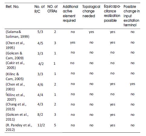
Table 1. Summary of Available Notch/All Pass Filters
The OTRA, as depicted in Figure 1, is a three terminal current mode analog device with two low-impedance input terminals and one low-impedance output terminal. The input terminals of the OTRA are virtually grounded. The input and output terminal of an OTRA can be characterized by the matrix of (1)
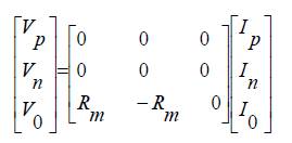
Where Rm is the transresistance gain of the ideal OTRA. Ideally, Rm value of the gain is very high, therefore the OTRA has to be used in negative feedback configuration for linear applications.
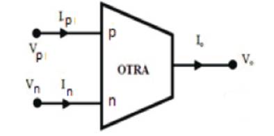
Figure 1. The OTRA Block
The CMOS based schematic of OTRA (Mostafa & Soliman, 2006) is shown in Figure 2. The transistors M1 – M13 form current differencing circuit and provide a virtual ground at p and n terminals whereas common source amplifier (M14) provides high gain.
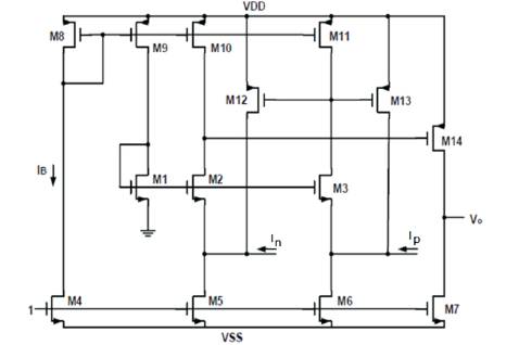
Figure 2. OTRA Block using CMOS Implementation (Mostafa & Soliman, 2006)
The proposed OTRA based notch/all pass filter is shown in Figure 3. It uses two OTRAs. The first OTRA provides an inverting band pass response, while the second one simply performs addition of the input signal and output of first OTRA.
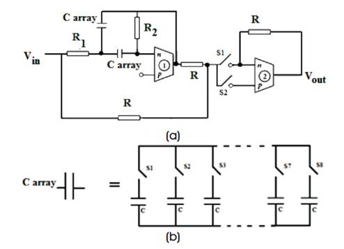
Figure 3(a). Proposed Second Order Notch/All Pass Circuit (b) C Array Implementation
The transfer function of the circuit of Figure 3 is computed as:
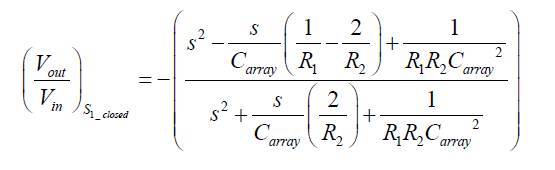
for switch S1 closed and,
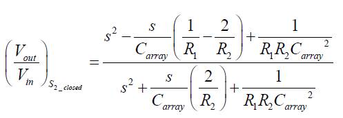
for switch S2 closed.
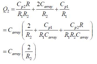
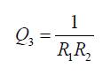
By choosing R2 =2R1 , the transfer functions of equations (2) and (3) reduce respectively to,
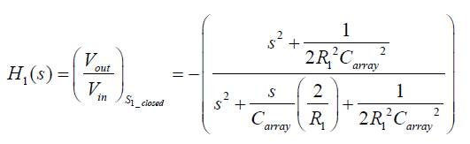
for switch S1 closed, and
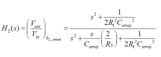
for switch S2 closed.
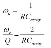
The transfer functions of equations (4) and (5) correspond to the inverting and non inverting notch filters and are characterized by the following pole frequency (ωo) and bandwidth 
With a selection of R2 =4R1 , equations (2) and (3) modify to
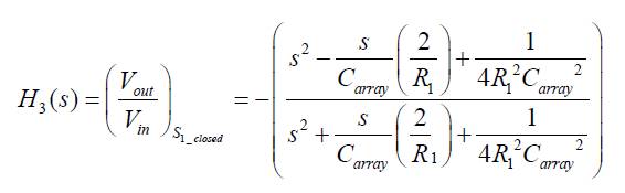
for switch S1 closed
and,
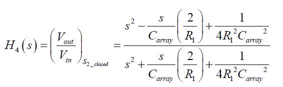
for switch S2 closed.
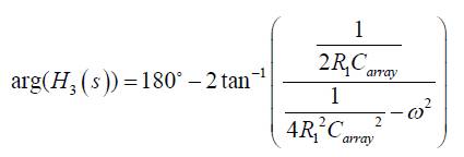
A close observation of equations (7) and (8) show that these transfer functions represent inverting and non inverting all pass responses, the argument of equations (7) and (8) are given by equations (9) and (10).
and,
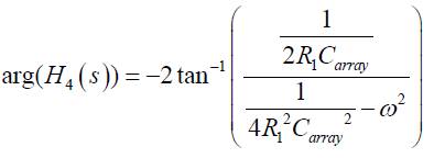
The phase of transfer function H3(s) changes from +180o to -180o whereas the variation for H4(s) is from 0o; through -180o to -360o.
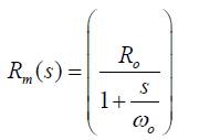
The transfer function in section 1 is derived by assuming infinite transresistance gain. The practical behavior of the active block, however, differs from ideal one. Practically Rm is a finite frequency dependant value. Considering a single pole model for the transresistance gain, Rm can be expressed as
For high frequency applications, the transresistance gain Rm (s) reduces to, Rm(s) 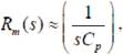
where 
Taking the finite trans impedance into account, the transfer function of equation (2), changes to
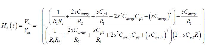
Transfer function equation (12) can be rewritten as,
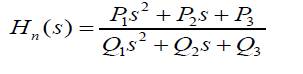
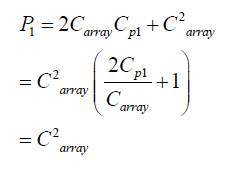
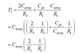
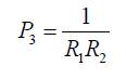
where
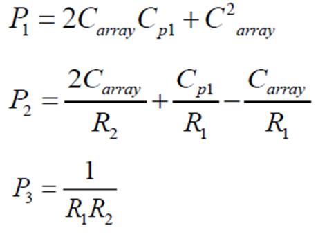
and,
Choosing the operating frequencies much below  and selecting external capacitors much higher than Cp∝ , that is, C array >>Cp∝ where a =1,2, the transfer function of equation (12) reduces to,
Similarly,
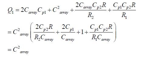
Substituting these values back in equation (13), we get
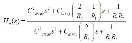
This is similar to equation (3) which is a non-inverting configuration. Therefore, the discussion of transfer function in section 2 remains valid for non - ideal case also.
The performance of the proposed notch/all pass filter of Figure 3 is verified through SPICE simulation using 0.5 μm CMOS technology parameters and power supply of ± 1.5V. The proposed notch filter is designed for ƒ0 = 80 KHz. The resistance values are chosen as R1= 2.1 kΩ, R2= 4 kΩ, and R= 4 kΩ, the capacitance C array is taken as 1nF. The magnitude and phase plots for H1(s) and H2(s) are plotted in Figures 4 and 5 respectively.
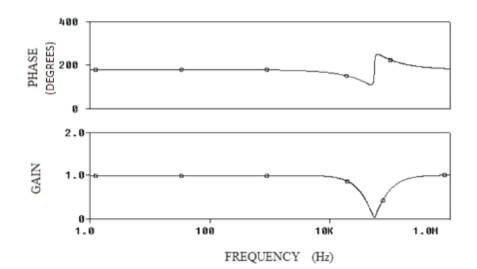
Figure 4. Phase and Magnitude Plot of Proposed Notch Filter (H1 (s))
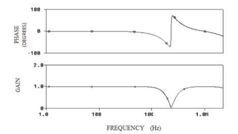
Figure 5. Phase and Magnitude Plot of Proposed Notch Filter (H2 (s))
The proposed all pass filter operation is verified for ƒ0 =80 KHz. The component values R1, R2 and R are taken as 0.25 kΩ,, 1 kΩ, and 4 kΩ, respectively. The capacitance is selected as 1nF. The magnitude and phase plots for H3(s) and H4(s) are placed in Figures 5 and 6 respectively. Figures 7 and 8 show the variation of phase of all pass filters by choosing different switch settings (Table 2) in the capacitor array.
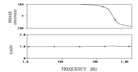
Figure 6. Phase and Magnitude Plot of Proposed All Pass Filter (H3 (s))
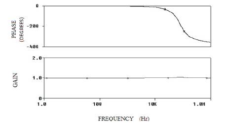
Figure 7. Phase and Magnitude Plot of Proposed All Pass Filter (H4 (s)))
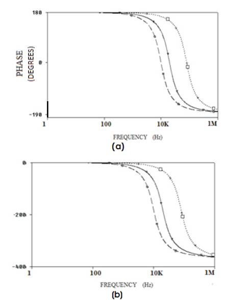
Figure 8(a). Phase Tuning of H 3(s) and 8(b) Phase Turning of H4 (s)
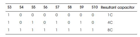
Table 2. Switch Settings in Capacitor Array
The all pass filter response is also obtained to check the effect of tolerance on all pass magnitude response. The number of runs is chosen as 20 and uniform deviation on resistors and capacitors are applied to the proposed all pass filter. Figure 9 shows the Monte Carlo SPICE simulation results for the gain of all pass filter for 100mV input.
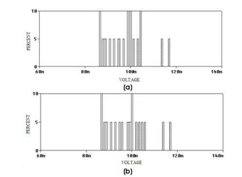
Figure 9. Monte Carlo Simulation Results for (a) H 3(s) and (b) H 4(s) for Tolerance on both Resistors and Capacitors
A new realization of the OTRA based second order notch/ all pass filter is presented. The proposed filter uses two OTRAs, five resistors and two capacitors implemented as capacitor array. It uses switches to provide electronic tunability and both inverting and non inverting responses. SPICE simulation results are included which corroborates with the theoretical predictions. Simulations were verified through CMOS based implementation of the OTRA which runs on 1.5V DC power supply and is based on 0.5 submicron technology. The frequency of the designed filter is 80 KHz and comfortable values for passive components have been selected. Phase tuning of the all pass filter has been done through the toggling of different capacitors using a capacitor array. Effect of tolerance has also been demonstrated through Monte Carlo analysis. By toggling the value of R1 between 0.25 kΩ, and 2.1 kΩ, we can extend the circuits capabilities to that of a second order all pass filter and a notch filter respectively.