Arithmetic and Logic Circuits are to be designed with less power, compact size, less propagation delay in this fast growing era of technology. Arithmetic operations are indispensable and the basic functions for any high speed low power applications like digital signal processing, microprocessors, image processing, etc. Consumption of power is the major issue in designing these circuits. Also the number of transistors required is also the one of the issues in designing the circuits. To minimize the transistors required in designing the circuits and to reduce the power consumption of the circuits, the authors have referred some techniques to overcome these problems in this paper. By reviewing all these techniques, the authors try to implement the GDI technique to reduce the power consumption and transistors count or the area required to design the circuits.
An Arithmetic and Logic Unit (ALU) is a digital circuit used to perform arithmetic and logic operations. It represents the fundamental building block of the Central Processing Unit (CPU) of a computer. Modern CPUs contains very powerful and complex ALU’s. In addition to ALUs, modern CPUs contain a Control Unit (CU) [3]. An ALU is a combinational circuit, meaning that its outputs will change asynchronously in response to the input changes. In a normal operation, stable signals are applied to all of the ALU inputs and, when enough time (known as the "propagation delay") has passed for the signals to propagate through the ALU circuitry, the result of the ALU operations appear at the ALU outputs. The external circuitry connected to the ALU is responsible for ensuring the stability of ALU input signals throughout the operation, and also for allowing sufficient time for the signals to propagate through the ALU before sampling the ALU result [5]. For every ALU working, the power required and the time required for its operation are also important traits. The transistor’s consuming area on the chip are also the important parameters while designing the ALU blocks. These parameters decide the working efficiency of ALU. In this paper, the study of different works of different authors has been mentioned and also to know how they have improved the functioning of ALU. In each paper, the authors have stated a different technique to modify the ALU design. The aim of this paper is to study these techniques and design the most reliable ALU. Working on the reduced power consumption of ALU, stops the leakage current which occurs in it. Also to minimize the number of transistors required in designing the different blocks in ALU, it directly affects the area required to mount the processors on chip [7]. So the authors try to design and implement the ALU by studying the GDI technique. In this paper, various methodologies of different authors, as well as the proposed GDI technique is explained.
ALU is a combination of various blocks. ALU is the core component of digital circuits, microprocessors, etc., which is used for both arithmetic and logical operations. ALU consist of CU, i.e, Control Unit which controls all the executions of the instructions inside a ALU [1]. ALU performs all the arithmetic operations like addition, subtraction, multiplication, and division in the arithmetic section. Similarly all the logical related operations like AND, OR, NAND, NOR, etc, are performed in logical section [3] . The basic block diagram of ALU is shown in Figure 1.
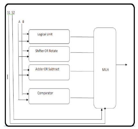
Figure 1. Basic Model of ALU Structure
In the logical unit of an ALU, various logical operations like NOT, AND, OR, NAND, NOR, XOR, XNOR, etc., are performed and executed. Logical Unit is one special unit made for these operations [2]. All logic operations are performed by using this logic unit. A MUX operated by select lines is used inside this logic block, which is used to perform a particular logic operation.
With the help of complementary logic a 1-bit comparator is used. By comparing the two I/Ps given, it gives three states of O/P for three different conditions [4]. In the barrel shifter, a 2:1 MUX is used as a cell, which is used for shifting and rotating operations in the comparator and shifter unit.
ALU is the most crucial and core component of CPU as well as embedded system and microprocessor. So, in this article, the authors designed have 4-bit ALU. The ALU determines the power consumption and operating speed of CPU. So, methods of reducing the power consumption and to improve the speed improvement have been discussed here.
In this paper, the author gives the importance to the power dissipation in designing the circuit, since this factor plays a major role in deciding the efficiency of the designed circuit. Power dissipation in turn reduces the whole power dissipation of CPU.
In this paper, the ALU is designed by using different technologies. ALU is the most crucial and core component of CPU as well as embedded system and microprocessor. So authors apply different techniques were used to design it [6].
In this article, author proposes ALU design using Reversible control unit (RCU) .It reduces the power dissipation to great extent in digital design.
In this paper Penman proposes four low power adder cells using different XOR and XNOR gate architectures.
In this paper the author tries to improve the performance of the ALU and reduce the cost required to build it.
Quantum Cellular Automata (QCA) is a nanotechnology system that has recently been recognized as one of the emerging technologies with potential applications in future computers [9].
Arithmetic Logic Circuits are to be designed with less power, compact size, less propagation delay in this fast growing era of technology [1]. Arithmetic operations are indispensable and basic functions for any high speed low power application digital signal processing, microprocessors, image processing etc.
Power dissipation is basically the power which is converted to heat and then conducted or radiated away from the device. Power dissipation in CPU can be reduced by considering the complete internal architecture of CPU and then reduce its power dissipation in different parts [3].CPU has two main parts CU and ALU. In this paper authors consider ALU.
The arithmetic logic unit (ALU) is the core of a CPU in a computer. The adder cell is the basic unit of an ALU. The constrictions are, adder has to satisfy area, power and speed requirements [4]. Some of the conventional types of adders are ripple-carry adder, carry-look ahead adder, carry-skip adder and Manchester carry chain adder. Macroscopic issues take time to market the design complexity (millions of gates) of high levels of abstraction for the design of test reuse and IP portability.
It has wide range of applications in advanced computing, low power CMOS design, and Optical information processing, in conventional CMOS design there is loss of some energy due to loss of some bits in logic operations [5]. So to overcome this author introduces Reversible logic gates.
The blooming development of Computer Science has led to the growth of integrated circuit (IC) devices [2] . Most of the Very Large Scale IC (VLSI) applications, such as digital-signal processing and microprocessors, use arithmetic operations extensively. In addition, among these, widely used operations are subtraction and multiplication and are most commonly applied [4]. The 1- bit full adder is the building block of these operation modules. Therefore enhancing its performance is crucial to ameliorating the performance of overall modules.
The International Technology Roadmap for Semiconductors (ITRS) is a group that came together with the objective to make the cost of semiconductor advancements more cost effective for IC (integrated circuits). They also have the size requirements for transistors that should be used in current IC [2] .
In this paper author proposes the novel technique to design the QCA adder [1]. The basic Boolean primitive in QCA is the majority gate. In this paper authors present a novel design for QCA cells and another possible and unconventional scheme for majority gates [4]. By applying these items, the hardware requirements for a QCA design can be reduced and circuits can be simpler in level and gate counts.
In this paper scribe uses the GATE DIFFUSION TECHNIQUE. Design of various cells in ALU like multiplexer, adder etc. is carried out in GDI technique [3]. The simulation of design is carried out by using Tanner EDA Tool in 250nmt technology.
In this paper scribe uses three different types of comparators which are Traditional comparator, Domino Style comparator and Pass Logic Based Single Stage Comparator [5]. In this paper, authors adapt strategy of differential clocking i.e. if parts of a device are made to work on either positive edge triggering or negative edge triggering then only half the circuit works at a given time and hence half of the circuit is inactive [7]. So the power dissipation factor reduces to half a time.
For designing the 1 bit ALU, evangelist use various methods which are 45nm, 65nm and 90 nm. And the performance of developed ALU has been analyzed and compared in terms of area and power using BSIM4 device model. The schematic of ALU circuit has been designed using DSCH 3.5 and its equivalent layout has been created using Micro-wind tool [2].
To reduce the power dissipation in digital design, scribe uses the Reversible Control Unit method. This Reversible ALU has been modeled and verified using Virolog and Quartus II 5.0 simulator. And Comparative results are presented in terms of number of gates, number of garbage outputs, number of constant inputs and Quantum cost.
In this paper authors used comparison between GDI developed gates and 3-transistors (3-T) XOR and XNOR gates .Simulations are performed by using H-spice based on 180nm CMOS technology.
In this paper, authors design the ALU using CPL and dual power supply design where one can accomplish energy and power leakage saving and gain a high throughput [4]. And also authors implement the QCA (Quantum dot Cellular Automata) full adder which makes the CPU design less complex.
In this paper, scribe constructs the 1-bit QCA adder by applying new QCA method and compares it with the existing one [1]. Also by using some Boolean functions and new reduction method, the decrease in gate count can be seen.
By using this method scribe reduces the power consumption of circuit much and it improves the speed of operation as the area required also gets reduced in it due to GDI technique [3].
Power dissipation is an important factor in determining the overall efficiency of circuits. In this paper by choosing appropriate circuit and clocking strategy one can minimize the problems associated with power dissipation.
It can be observed from simulation results that 45nm technology based ALU has shown area reduction ranging from 48 % to 75% with 65nm and 90nm technology and power reduction from 84% to 97.9% as compared with 65nm and 90nm based technologies.
In this method scribe uses six parameters to determine the complexity and performance of circuit that are gates count, garbage output, constant input and quantum depth.
The proposed four full adder cells demonstrate their advantages, including lower power consumption, smaller area, and higher speed.
Energy and Area Analysis of a Floating-Point Unit is given by 2.048mW (45nm) 0.6340mW (15nm) and Ultra-areaefficient fault-tolerant QCA full adder is low.
The QCA adder has been compared with another existing implementation of QCA adders [4]. It is simply that proposed item reduces the level counts and the put majority and inverter.
GDI cell proposed by Morgenshtein is shown in Figure 2 for designing the low power combinational circuit GDI which is a proposed approach [2]. This approach leads to reduction in power consumption, propagation delay and area of digital circuits is obtained when the complexity of logic design is low [3]. Under certain operating conditions, it provides in-cell swing restoration, because basically this is a two transistor complex logic function [5]. The special feature of GDI is that, source of PMOS is not connected to VDD, and source of NMOS is not connected to GND. So GDI provides two extra input pins for use which makes it more flexible than CMOS design.
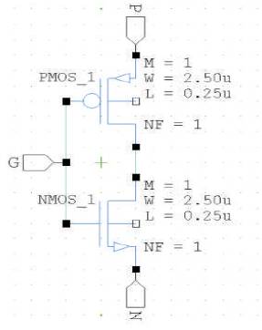
Figure 2. Basic GDI Cell
In GDI cell Voltage drop will get restored due to buffers being added and buffers are assisted with power supply. GDI is the new approach for designing the low power combinational circuit. By using this approach, it leads to power consumption reduction, propagation delay and area of digital circuits are obtained when the logic design complexity is low. Under certain operating conditions, it provides in-cell swing restoration, because basically this is a two transistor complex logic function. Source of PMOS is not connected to VDD and source of NMOS is not connected to GND, and this is the special feature of GDI.
The tool which is used for simulation in this paper is Tanner ED.
There are many phases or progressions of a design. A common term heard when working with a Designer is “Schematic Design”. This phase is early in the design process. Schematic Design establishes the general scope, conceptual ideas and the scale and relationship of the various program elements. The primary objective of schematic design is to arrive at a clearly defined feasible concept based on the most promising design solutions.
The Layout Versus Schematic (LVS) is the class of EDA verification software that determines whether a particular integrated circuit layout corresponds to the original schematic or circuit diagram of the design. LVS checking software recognizes the drawn shapes of the layout that represent the electrical Components of the circuit, as well as the connections between them. This netlist is compared by the "LVS" software against a similar schematic or circuit diagram's netlist.
After schematic design it checks whether design match with the specification is required or not. That's why authors need to simulate the design which is called Pre layout simulation.
A layout-design of an IC refers essentially to the 3- dimensional character of the elements and interconnections of an IC. There is a continuing need for the creation of new layout designs which reduce the dimensions of existing integrated circuits and simultaneously increases their functions.
Design Rule Check (DRC) is the area of Electronic Design Automation (EDA) that determines whether the physical layout of a particular chip layout satisfies a series of recommended parameters called Design Rules. Design rule checking is a major step during Physical verification sign off on the design [6]. Design Rules are a series of parameters provided by semiconductor manufacturers that enable the designer to verify the correctness of a mask set. Design rules are specific to a particular semiconductor manufacturing process.
The aim of this review is to get readers the basic and essential knowledge regarding ALU by studying these papers, and to know the various methods for designing the ALU. The main trait in designing the ALU is its power consumption and area required. Authors get the various technology to reduce it by studying these papers. But authors find that GDI is more convenient and try to reduce the power consumption and area required for ALU by designing it in GDI technology.