Energy-efficiency is one of the most required features of modern electronic systems designed for high-performance and/or portable applications. Now-a-days the need for having greater computing power based on battery operated mobile devices is increasing. For this, instead of optimizing the conventional delay time and area size, it is also required to minimize the power dissipation while still maintaining the high performance. An adder is an important element of all the arithmetic and logic units. The recent trends in VLSI are moving towards the need of the devices, which consume low power. Binary adders are one of the most basic and widely used in arithmetic operations. Full-adder is the fundamental unit to carry out the addition. Numerous logics have been proposed in the literature to implement full adder using MOS transistors, namely Pass transistor logic, Double pass transistor logic, DVL, CPL, etc.
Full-adder implementing with a DPL logic style uses XOR/XNOR gates, and a pass-transistor based multiplexer to obtain the Sum (S ) output, and SR-CPL logic style uses only XOR/XNOR gates. In both cases, the AND/OR gates are build using a powerless and groundless pass-transistor configuration, respectively, and pass-transistor based multiplexer to get the Carry (C ) output. In this paper, DPL (Proposed Method), and SR-CPL are implemented using PSPICE software, among them SR-CPL shows better performance in Power Dissipation and it occupies less area in IC.
Low power design directly leads to prolonged operation time in these portable devices. Arithmetic circuits, like adders and multipliers, are one of the basic components in the design of communication circuits. Recently, an overwhelming interest has been seen in the problems of designing digital systems for communication systems and digital signal processing with low power at no performance penalty. Designing low power high-speed arithmetic circuits requires a combination of techniques at four levels; algorithm architecture, circuit and system levels.
Minimizing power consumption for digital systems involve optimization at all levels of the design. This optimization includes the technology used to implement the digital circuits, the circuit style and topology, the architecture for implementing the circuits and at the highest level, the algorithms that are being implemented. The most important technology consideration is the threshold voltage and its control, which allows the reduction of supply voltage without significant impact on logic speed. Since energy is consumed only when capacitance is being switched, power can be reduced by minimizing this capacitance through operation reduction, choice of number representation, exploitation of signal correlations, resynchronization to minimize glitching, logic design, circuit design, and physical design.
After guaranteeing correct digital functionality, the primary consideration for the system designers is speed. A circuit is specified to operate at a particular delay, otherwise the entire system may not work; further reduction is beneficial, but not strictly necessary. Other factors may have equal or greater importance than power dissipation; area of implementation and reliability issues are the subjects which a designer must take into account. It's worth to note that power reduction techniques are not necessarily negatively correlated to delay reduction. However, reducing interconnect capacitance, which is another way to lower delay, reduces both power and delay. Generally, great power savings can be achieved if delay is not an issue, but optimizing power without delay consideration is insignificant.
Addition is the most common and often used arithmetic operation on microprocessor, digital signal processor, especially digital computers. Also, it serves as a building block for synthesis of all other arithmetic operations. Therefore, regarding the efficient implementation of an arithmetic unit, the binary adder structures become a very critical hardware unit.
In this paper, qualitative evaluations of the classified binary adder architectures are given. Among the huge member of the adders PSPICE (Simulation Program with Integrated Circuit Emphasis) code is written for CMOS conventional full adder, Dual Value Logic adder (DVL), Complimentary Pass transistor Logic adder (CPL), Static Differential Cascade Voltage switch full adder (SDCV), Static Energy Recovery Full adder (SERF) to emphasize the common performance properties [3].
Apart from these adders, the codes for two new fulladders have been designed using the logic styles DPL and SR-CPL and the new logic structure presenting here which are going to have less power dissipation, less number of transistors and high output voltage. In the following section, a brief description of the studied adder architectures or previous different logic styles and logic structures used to build the adder module has been given.
Conventional CMOS has proved to be functional and efficient at ultra low voltage even though the pMOS logic tree is redundant and increases the total amount of switch capacitance per gate [1]. It is used in most of the chip designs in the recent VLSI applications. Conventional CMOS is very efficient for basic inverting gates such as AOI, OAI, and NAND.
In order to obtain a reasonable conducting current to drive capacitive loads, the width of the transistors must be increased [2]. This results in increased input capacitance and therefore high power dissipation and propagation delay. In this CMOS, the voltage swing at the output nodes is equal to the supply voltage resulting in high power dissipation.
Conventional CMOS full adder is as shown in Figure 1. Here for AND operation, nMOS are connected in series and pMOS are connected in parallel and for ORing operation, nMOS are connected in parallel and pMOS are connected in series [4].
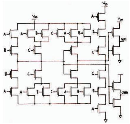
Figure 1. Conventional CMOS Full Adder
The main concept behind Complementary Pass Transistor Logic (CPL) is the use of only an nMOS network for the implementation of logic functions. This results in low input capacitance and high speed operation because the high voltage level of the pass transistor output is lower than the supply voltage level by the threshold voltage of the pass transistors, the signal have to be amplified by using CMOS inverters at the outputs.
A CPL circuit consumes less power than the conventional static circuits because the logic swing of the pass transistor outputs is smaller than the supply voltage level. To minimize the static current due to the incomplete turn off of the pMOS in the output inverters, a weak pMOS feedback device can also be added in the CPL circuits in order to pull the pass transistor output to full supply voltage level. However, this will increase the output node capacitance leading to higher switching power dissipation and higher propagation delay [3].
CPL is a voltage restricted logic style. The voltage drop due to the threshold voltage of MOS transistors can be an important feature in CPL logic style. In CPL, the level high of the logic tree is Vdd-Vt, since, the trees are made of nMOS transistors only. Its output is buffered with an inverter to bring the level high to Vdd. Hence the high before the inverter must be greater than Vdd/2. So that the inverter buffer can actually amplify the level high instead of attenuating it [2].
This explains why CPL can only operate for Vdd greater than twice Vt.
The circuit diagram of CPL is as shown in Figures 2 (a) and (b).
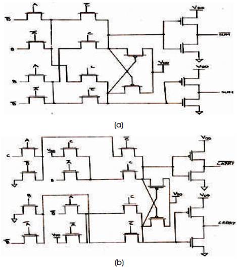
Figure 2 (a) CPL logic for sum, (b) CPL Logic for Carry
Static Differential Cascode Voltage Switch Full adder (DCVSL), is a differential style of logic requiring both true and complementary signals to be routed two gates. Figures 3 (a) and 3 (b) show the circuit diagram of the DCVSL full adder, where two complementary responding nMOS switching trees are constructed to a pair of cross coupled pMOS transistors depending on the differential inputs and one of the output is pulled down by the corresponding nMOS [5]. The differential output is then latched by the cross coupled pMOS transistors. Since the inputs drive only the nMOS transistors of the switching trees, the input capacitance is typically two or three times smaller than that of conventional CMOS logic [7] .
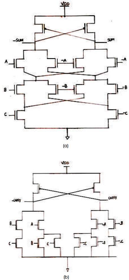
Figure 3 (a & b) Static Differential Cascaded Voltage Switch Full Adder
Double Pass Transistor Logic is a modified version of CPL. The circuit diagram of the DPL full adder is shown in Figure 4. In DPL circuit, full-swing operation is achieved by simply adding pMOS transistors in parallel with the nMOS transistors. Hence the problems of noise margin and speed degradation at reduced supply voltages are caused in CPL circuits due to the reduced high voltage level, are avoided. However, the addition of pMOS results in increased capacitances.
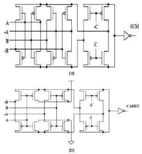
Figure 4 (a) DPL Logic for Sum, (b) DPL Logic for Carry
But CPL circuit consumes less power than DPL one, because of its low parasitic capacitances. DPL circuit is faster than CPL, because of pMOS transistors in parallel with the nMOS transistor that results in higher circuit drivability. Also, DPL avoids the problems of noise margin and speed degradation at reduced supply voltages which are caused in CPL circuits [7].
Dual Value Logic (DVL) is the lower power logic circuit style and it has similar characteristics and is usually included within conventional CMOS standard cells, as it efficiently implements the MUX and XOR type functions as shown in Figure 5. DVL relies on simplification of the redundant paths with a careful synthesis methodology. In DVL none of the internal nodes need to be buffered and this property makes this logic a potential candidate for ultra low voltage operation [6]. However, the major issue in pass gate logic synthesis is the irregular nature of the input capacitances within a single gate. DVL presents the problems of long device stacks or chains during synthesis. The common solution is to buffer all the drain or source inputs with the inverters for every cell. Unfortunately this leads to less efficient design due to the overload of all the inverters [3].
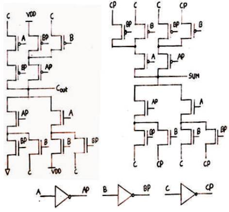
Figure 5. Dual Value Logic Adder
Examing the full-adder's truth-table in Table 1, it can be seen that the So output is equal to the  value when C=0, and it is equal to
  when C=1. Thus, a multiplexer can be used to obtain the respective value taking the C input as the selection signal. Following the same criteria, the Co output is equal to the A • B value, when C=0, and it is equal to A+B value, when C=1. Again, C can be used to select the respective value for the required condition, driving a multiplexer. Hence, an alternative logic scheme to design a full-adder cell can be formed by a logic block obtain the and signals, another block to obtain the A • B and A+B signals, and two multiplexers being driven by the C input to generate the Sum (So) and Carry (Co) outputs, as shown in Figure 6.
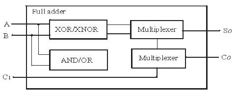
Figure 6. Alternative Logic Scheme for Designing Full-adder Cells
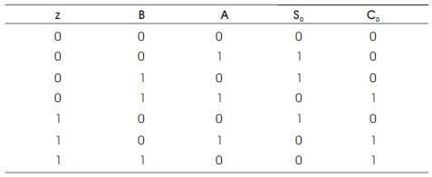
Table 1. Truth Table for a 1-Bit Full-adder
The features and advantages of this logic structure are as follows.
Based on the results obtained in the above full adder cell, two new full adders have been designed using the logic styles DPL (Proposed) and SR-CPL. Figure 7 presents a full adder designed using a DPL (Proposed) logic style to build multiplexer to obtain the So output. In Figure 8, the SR-CPL logic style was used to build these XOR/XNOR gates. In both cases, the AND/OR gates have been built using a powerless and ground less pass transistor configuration, respectively, and a pass-transistor based multiplexer to get the Co output.
Double Pass Transistor Logic (DPL) is a modified version of CPL. The new full adders have been designed using the logic style DPL and new logic structure is shown in Figure 7. The AND/OR gates have been built using a powerless and groundless pass transistor configuration, and a passtransistor based multiplexer to get the Co output. In DPL circuit, full- swing operation is achieved by simply adding pMOS transistors in parallel with the nMOS transistors. Hence the problems of noise margin and speed degradation at reduced supply voltages caused in CPL circuits due to the reduced high voltage level, are avoided. However, the addition of pMOS results in increased capacitances.
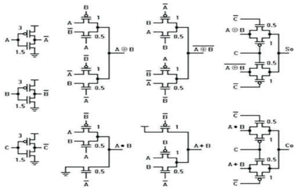
Figure 7. Full-adder designed with the Proposed Logic Structure and a DPL Logic
DPL circuit is faster than CPL, because of pMOS transistors in parallel with the nMOS transistors results in higher circuit drivability. Also, DPL avoids the problems of noise margin and speed degradation at reduced supply voltages which are caused in CPL circuits.
Swing restored Complementary Pass Transistor Logic (SRCPL) is a modified version of CPL. The new full adders have been designed using the logic style and SR-CPL new logic structure is shown in Figure 8. Figure 8 presents a full-adder designed using a SR-CPL logic style to build the XOR/XNOR gates to obtain the So output.
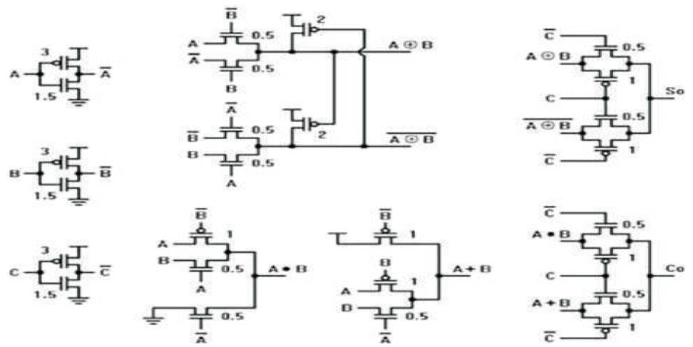
Figure 8. Full-adder Designed with the Proposed Logic Structure and a SR-CPL Logic Sytle
The AND/OR gates have been built using a powerless and groundless pass transistor configuration, and a passtransistor based multiplexer to get the Co output. In SR-CPL circuit, full-swing operation is achieved by simply adding pMOS transistors in parallel with the nMOS transistors [7]. Hence the problems of noise margin and speed degradation at reduced supply voltages caused in CPL circuits due to the reduced high voltage level, are avoided. However, the addition of pMOS results in increased capacitances.
But SR-CPL circuit consumes less power dissipation than CPL and DPL one, because of its low parasitic capacitances. DPL circuit is faster than CPL, because of pMOS transistors in parallel with the nMOS transistor results in higher circuit drivability. Also, SR-CPL avoids the problems of noise margin and speed degradation at reduced supply voltages which are caused in the CPL circuits.
Among many simulation softwares on the market, PSPICE has various advantages:
The professional version of PSPICE is far too expensive for most of us. But fortunately there is a demo version which is completely free and easily obtainable [8].
A demo version is always limited, of course, but here the limit is only in the number of connections which one can simulate. All the other features are available.
The use of a simulation software is an essential requirement.
The following steps are needed to simulate a circuit from the PSPICE A/D application:
The CCMOS, DPL (Existing method), CPL, DPL (Proposed Method), SR-CPL Logic styles are simulated using PSPICE software and the Power dissipation, and area were compared as given in Table 2.
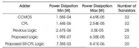
Table 2. Comparison of Various Parameters
The simulation environment is used for comparing the existing method with DPL (Proposed), and SR-CPL Fulladders. In order to demonstrate its advantages, two new full-adders were built in combination with pass transistor powerless/groundless logic styles. Among them, SR-CPL has very less power dissipation and the number of transistors are reduced too. The MINIMUM and MAXIMUM power dissipation of SR-CPL is 7.38 E-06 W to 7.41 E-06 W. To build SR-CPL, only 20 transistors are required.
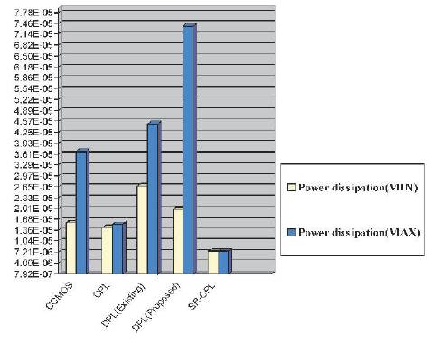
Figure 9. Power Dissipation of Various Adder Cells
Figure 9 represents the power dissipation of various adder cells [10]. This illustrates that the DPL (Proposed) adder cell is having the highest power dissipation, i.e., 7.38 E-05 W (high), 1.98E-05 W (low) and the proposed SR-CPL adder cell is having the less power dissipation i.e., 7.41 E-06 W (high) and 7.38 E-09 W (low).
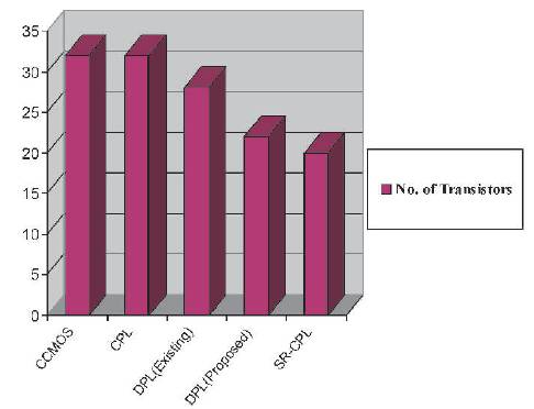
Figure 10. The number of Transistors of Various Adder Cells
Figure 10 represents the number of transistors present in various adder circuits. This illustrates that the conventional CMOS full adder is having the highest number of transistors i.e., 32 and the proposed SR-CPL adder cell is having the less number of transistors, i.e., 20. As the number of transistor minimizes, the complexity of the circuit will be reduced, which in turn decreases the area. This is very beneficial in modern IC technology.
This paper is aimed to design and simulate an SR-CPL fulladder. SR-CPL has less power dissipation compared to the existing methods of full adders and also it requires less number of transistors, so that it occupies a lesser area in IC.
SR-CPL is used for low power operated circuits (i.e, portable devices), hence “CMOS Full-adder For Energyefficient Arithmetic Applications” is good in mainly in two aspects, viz. less Power dissipation, and less area. Energy is consumed only when capacitance is being switched, power can be reduced by minimizing this capacitance through operation reduction, choice of number representation, exploitation of signal correlations, resynchronization to minimize glitching, logic design, circuit design, and physical design.
The adder is a main component in multiplier circuits. By optimizing an adder cell for less propagation delay, less area, low power consumption that will lead to better performance of a multiplier can be implemented.
As the SR-CPL logic style for a full adder is very efficient for low power and less area applications, this can be used in multipliers, data path operator, etc., to improve their overall performances.