Operational Transresistance Amplifier (OTRA) is an inherently suitable active building block for analog VLSI applications, since the OTRA is not slew limited in the same fashion as voltage op amps [2]. It can provide a high bandwidth independent of the gain. Hence, it does not suffer from constant gain bandwidth product like voltage op amps circuits [8]. An Operational Transresistance Amplifier (OTRA) based phase detector circuit has been proposed, due to the fact that both input and output terminals of OTRA are characterized by low impedance. The proposed circuit is simple to realize and consists of two OTRA based comparators, a CMOS XOR circuit, buffer and an RC integrator.
The Clock and Data Recovery (CDR) circuit is an integral part of high-speed serial data communication systems and phase detectors play an essential role in CDR circuits [1]. The PD outputs a control signal, dependent upon the phase difference between an input reference and a Voltage-Controlled Oscillator (VCO), which is used to vary the VCO frequency [5]. Extensive literature review suggests that the existing PD circuit design approaches can broadly be classified as those based on digital [9-12] and analog [3,13] techniques. The PD designs proposed in [3,9,10,12] are binary circuits and are suitable for random phase detection. The PD circuit presented in [12] is a tri-state binary PD design having phase response similar to that of the PD proposed in [4], however, this PD circuit is more robust against process non-idealities [12]. A highfrequency, low power Phase-Locked Loop (PLL) in bipolar technology has been proposed in [14] using a varactortuned voltage controlled oscillator, an analog phase detector, and a band gap reference as building blocks. Two configurations of cascadable phase sensitive detectors have been proposed in [3], which allow the realization of any phase response by cascade or parallel connections of similar stages. To generate a phase discrimination response with a specified sensitivity and detection range, a mathematical procedure is proposed in [15] and an algorithm is developed to synthesize it using an analog multiplication, programmable coefficient scaling, and transversal summing. To the best of authors' knowledge, no PD circuit design based on Analog Building Blocks (ABB) is available in literature.
Ever since its development, the operational amplifier (opamp) is an integral part of analog signal processing and generating circuits. It is intended to implement closed loop voltage processing circuits which are known as Voltage- Mode (VM) circuits. However, high frequency performance of these circuits is limited due to constant gain-bandwidth product and low slew rate of the op-amps. The attempt to overcome this problem has led to the development of Current-Mode (CM) signal processing. In CM signal processing, current is used as the active variable in preference to voltage, either throughout the circuit or only in certain critical areas [7].
Therefore this paper aims at presenting an OTRA based phase detector using a simple scheme. The OTRA being a current mode device, its bandwidth is independent of the closed loop gain. In addition, it is free from parasitic input capacitances and resistances making it suitable for high frequency applications.
The paper is organized as follows: In section 1, the phase detectors introduction is briefly described. Section 2 describes the basic building blocks used as comparator.
Section 3 describes the proposed system. In section 4, CMOS realizations of OPAMP and OTRA are given. In section 5, the simulation results of the proposed circuit has been presented and finally, the last section concludes the paper.
Phase Detectors (PDs) are important components of Phase Locked Loops (PLLs) for digital and analog applications. The PD outputs a control signal, dependent upon the phase difference between an input reference and a Voltage Controlled Oscillator (VCO), which is used to vary the VCO frequency.
Phase detectors generally appear in two different forms. Non-linear PDs coarsely quantize the phase error, producing only a positive or negative value at their output. Linear PDs, on the other hand, generate a linearly proportional output that drops to zero when the loop is locked. Based on their characteristics, phase detectors can be broadly categorized into (i) Combinational PDs, (ii) XOR PDs, and (iii) Edge-triggered PDs [2]. Now a new approach has been proposed in designing of phase detectors using CMOS OTRA as comparator [6], which is compared with CMOS OPAMP comparator.
An operational amplifier is a direct-coupled high-gain amplifier usually consisting of one or more differential amplifiers. The operational amplifier is a versatile device that can be used to amplify DC as well as AC input signals and was originally designed for performing mathematical operations.
The output of comparator shown in Figure 2, is high (VDD) when the difference between the non inverting and inverting input is positive, and low (VSS) when this difference is negative. Figure 1 represents the comparator symbol.
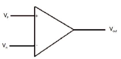
Figure 1. Comparator Symbol
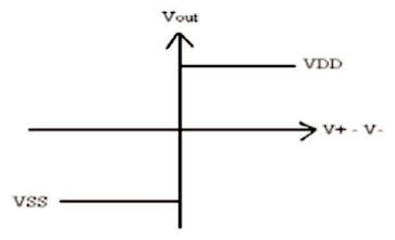
Figure 2. Output of Comparator
The Operational Transresistance Amplifier (OTRA) is a threeterminal analog building block. OTRA is a high gain current input voltage output device. The circuit symbol of OTRA is shown in Figure 3 and the port characteristics are given by equation (1), where Rm is transresistance gain of OTRA. For ideal operations, the Rm of the OTRA approaches infinity and forces the input currents to be equal.
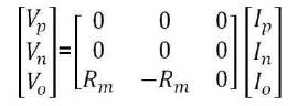
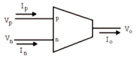
Figure 3. OTRA Circuit Symbol
The input and output terminals of the OTRA are characterized by low impedance, thus the response limitations incurred by capacitive time constants can be ignored [2, 7].
The proposed circuit is simple to realize and consists of two OTRA based comparators, a CMOS XOR circuit and an RC integrator.
A PD circuit is a 3-port configuration [3] as shown in the block diagram of Figure 4. A sinusoidal signal Vref of frequency ω is applied as a reference signal to input port 1 of the phase detector. A test signal Vtest of same frequency as that of Vref , with an instantaneous phase deviation (Φ) would be obtained from the output Port 3 [3].
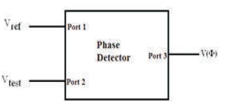
Figure 4. Block Diagram of PD
The OTRA based PD is shown in Figure 5. It consists of two OTRAs, a CMOS XOR circuit and an RC integrator. To interface the XOR gate with the integrator, a buffer circuit is used so that the loading effect of the integrator can be avoided. Both the OTRAs are used in open loop configuration to work as comparators.
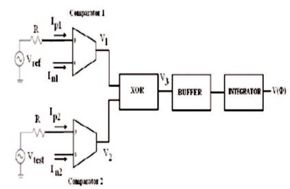
Figure 5. Proposed PD Circuit
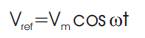
A reference sinusoidal is applied to the comparator 1 and comparator 2 is driven by another sinusoidal signal whose phase is to be detected. Considering a sinusoidal signal to be applied at comparator 1 is represented as,
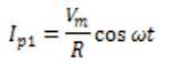
The current Ip1 through p terminal of OTRA1 is given by,
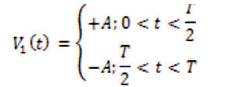
The current In1 for OTRA 1 being zero, the output of the comparator 1 will be at positive saturation level +Vsat for positive half cycle of Vref . However, during the negative half cycle of input voltage, the output will saturate at –Vsat . Thus comparator 1 provides a periodic rectangular output. Representing ±Vsat by ±A, the output of the comparator can be expressed as,
An another sinusoid of same frequency, delayed in phase by an angle φ is applied to the comparator 2 which can be expressed as,

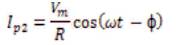
The current Ip2 through p terminal of OTRA 2 can be computed as,
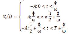
Since In2 is zero, the output of comprator 2 will be similar as that of output of comparator 1 but delayed in time by  and can be expressed as,
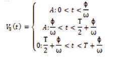
The outputs of the two comparators serve as input to the XOR gate. The XOR gate provides a pulsed output of period and can be represented as,
The output of the XOR Gate is integrated to obtain V(φ), which is the output of the proposed phase-detector and can be expressed as,
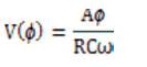
Using equation (9), the integrator output V(φ) can be computed for any phase delay (φ). It clearly shows that V(φ) is proportional to the phase delay of the applied sinusoidal signal. Hence, it is clear that the proposed PD produces an output voltage proportional to the phase delay of the applied sinusoidal signal.
It consists of 8 transistors with respective aspect ratios as given in Table 1. The n-channel transistors M1 and M2 form the input differential pair, and the p-channel transistors M3 and M4 form the active load. The diff-amp input stage is biased by the current mirror M5 and M6, in which the reference current is supplied by Ibias which is 30uA. The second stage, which is also the output stage, consists of the common-source connected transistor M7. Transistor M8 provides the bias current for M7 and acts as the active load. An internal compensation capacitor is included to provide stability. Figure 6 shows the CMOS OPAMP Implementation.
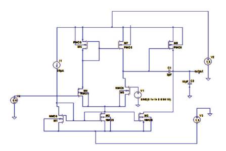
Figure 6. CMOS OPAMP Implementation
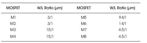
Table 1. Aspect Ratios of OPAMP of Figure 6
This section describes the OTRA implementation with their aspect ratios as given in Table 2, used to verify the functionality of all the circuit structures proposed in this thesis. The CMOS based OTRA structure proposed in [2] has been reproduced in Figure 7. The circuit operation is based on the assumptions that all the transistors (M1- M14) operate in saturation region and the transistor groups (M1- M3), (M5 and M6), (M8-M11) and (M12 and M13) are perfectly matched. Transistors M8-M11 form current mirror wherein the transistor M8 sets the reference current I B which is repeated by M9-M11thus forcing equal currents in the transistors M1, M2 and M3. This provides the gate to source voltages of M1, M2 and M3 and, consequently, forces the two input terminals to be virtually grounded. The current mirrors formed by the transistor pairs M10-M11 and M12- M13 provide the current differencing operation, thus developing gate to source voltage for M14, which is connected as a common source amplifier and provides the high gain.
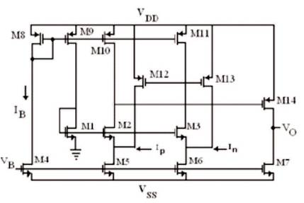
Figure 7. CMOS Implementation of OTRA [4]
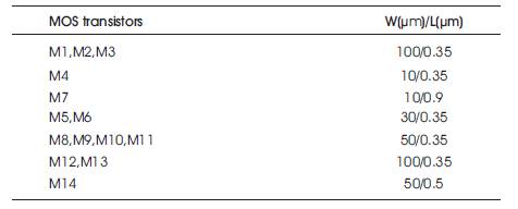
Table 2. Aspect Ratios of OTRA of Figure 7
Figure 8 shows the simulation results of the two stage opamp as comparator is compared with OTRA. The input frequency for these simulations is 1KHz.
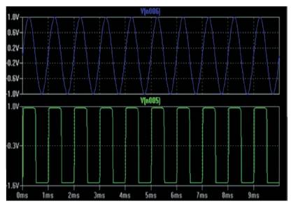
Figure 8. OPAMP Input and Output Waveforms
The work ability of the proposed OTRA based phase detector circuit is verified through SPICE simulations using 0.35μm CMOS process parameters. The CMOS implementation of the OTRA proposed is used. Supply voltages are taken as ± 1.5V. The Vref is taken as 1V, 1KHz signal as shown in Figure 9.
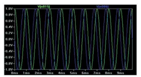
Figure 9. OTRA Input Voltage Waveforms
The corresponding input current Ip1 is shown in Figure 10. The comparator 2 is also driven by a similar sinusoid having phase delay φ=90° respectively. The resulting input current Ip2 for different phase delays is shown in Figure 10.
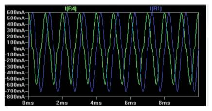
Figure 10. Input signals to Phase Detector: Ip1 with φ=0° , Ip2with φ=90°
The outputs of comparator 1 and comparator 2 for the applied inputs are shown in Figure 11(a), Figure 11(b), Figure 11(c) and Figure 11(d) respectively, whereas the output of XOR gate is shown in Figure 12. The integrator components are chosen as R=5KΩ and C=5 μF. It can be observed from Figure 13 that with increasing phase delay (i), the duration of the output waveform of the XOR gate increases. The simulated output pulse duration for φ= 30°, φ= 60° and φ= 90° were observed to be 85.578 μs, 168.1 μs and 253.595 μs respectively. The simulated power dissipation of the proposed circuit is 57 μw.
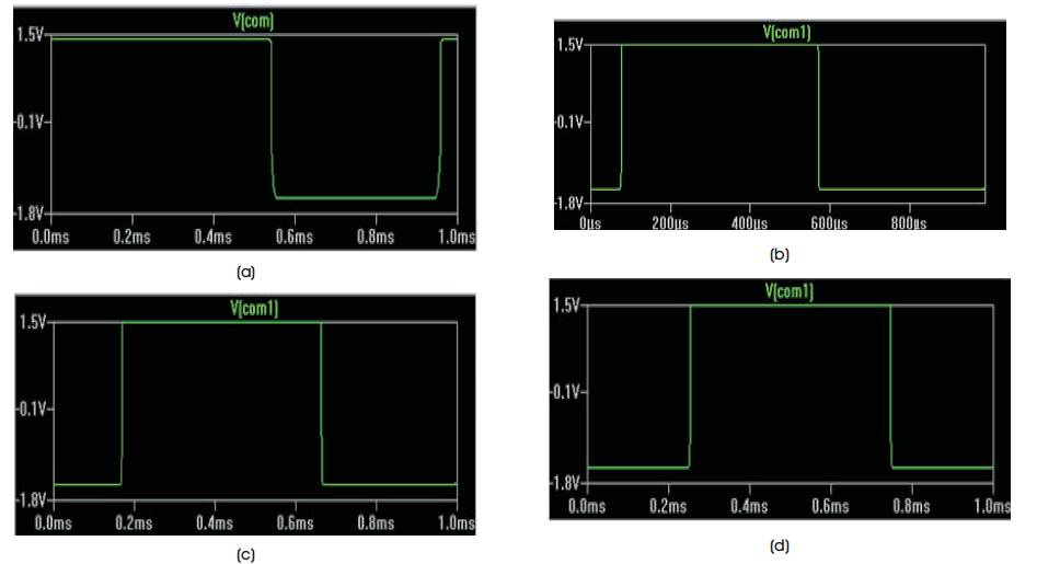
Figure 11. Output Waveforms (a) Comparator 1with φ=0°, (b) Comparator 2 with φ=30°, (c) Comparator 2 with φ=60°, (d) Comparator 2 with φ=90°
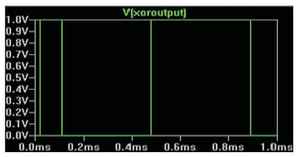
Figure 12. XOR Output Waveform
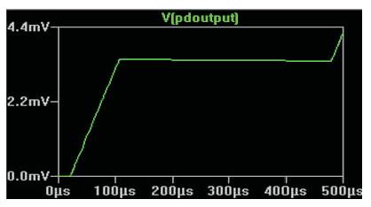
Figure 13. Phase Detector Output Waveform
The output of the proposed PD V(φ), as obtained by integrating the XOR output is shown in Figure 13.
The simulated and theoretically calculated values of V(φ) for different phase angles are listed in Table 3. It may be noted from Table 3 that the output voltage V(φ) increases linearly with the increase in phase delay.
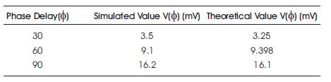
Table 3. Output Voltages
Phase detectors play an essential role in CDR circuits to recover clock and data. In this paper, an Operational Transresistance Amplifier (OTRA) based phase detector circuit has been proposed. The proposed circuit is simple to realize and consists of two OTRA based comparators, a CMOS XOR circuit, buffer and an RC integrator. The proposed circuit consists of OTRA as comparator has many advantages against OPAMP like being a current mode device, and its bandwidth is independent of the closed loop gain. In addition, it is free from parasitic input capacitances and resistances making it suitable for high frequency applications. The workability of the proposed circuit is verified through SPICE simulations and the simulated results are found to be in conformity with the theoretical formulation.