In this modern era, the challenge for IC designers is to maintain a prolonged battery lifetime in portable devices as power consumption is soaring with increased functionality and operating frequency. Excessive power consumption is the major barrier to the advancement of nanoscale CMOS VLSI circuits. Leakage currents are important sources of power consumption in sub-nanometre regime designs. The main sources of leakage are sub threshold leakage, gate leakage, gate induced drain leakage and junction leakage. Sub threshold leakage is the major contributor of static power and minimizing this component is more important in order to alleviate static power. The portable electronic gadgets like smartphones, tablet computers, etc., generally has much longer stand-by period than the operating period. Therefore an increased stand-by current wastes battery power seriously due to leakage. Power gating techniques help to minimize the leakage currents and increase the performance of integrated circuits. The basic strategy of power gating is to provide two power modes, a sleep mode and an active mode. The goal is to switch between these modes at the appropriate time and in the appropriate manner to maximize power savings while decreasing the impact to performance. This paper gives an overview of power gating techniques for controlling static power dissipation and retaining data in stand by periods.
Dynamic and static power consumption contributes the average power consumed by CMOS circuits. Previously, the major concern of chip designers is dynamic power consumption as it accounted for about 99% of the total chip power. Static power consumption dominates total chip power as technology scales down ( Taur 2002). Static power has become a critical issue in battery powered hand held devices, as their battery power will be drained off if they remain idle for a long time ( Rabeay 1996, Kao et al. 2002 , Keating et al. 2007). This necessitates the need to orient the research towards reducing static power dissipation in VLSI circuits. In this paper, a brief survey of techniques have been proposed to minimize power consumption.
The remainder of the paper is organized as follows, section 1 describes about the techniques to reduce leakage and section 2 briefs the literature survey of power gating techniques. Simulation results are discussed in section 3 and finally the paper is concluded.
Static power has four main components, sub-threshold leakage, gate leakage, gate induced drain leakage and reverse bias junction leakage. Sub threshold leakage is the main contributor of static power consumption in CMOS circuits ( Roy and Sharat, 2007, Weste and David, 2010). Dependence of sub threshold leakage on threshold voltage is given by,
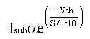
Where Vth is the threshold voltage of MOS transistor and S is the sub threshold swing. Equation (1) shows that leakage current increases exponentially as threshold voltage decreases. Hence, deep sub-nanometer technologies suffer from high leakage due to low threshold voltages in this regime. Following circuit techniques are developed for reducing the impact of leakage and to extend the battery life in portable devices while maintaining performance.
Multi-VT : Using high VT cells in circuit blocks wherever performance goals allow and low VT cells where necessary to meet timing ( Liao et al. 2002).
Power Gating: Shutdown the power supply to a circuit block of logic when it is not active.
VTCMOS: Reducing the value of the term (VGS -VT ) effectively, by applying a reverse bias voltage to the substrate ( Singh et al. 2007. ).
Stack Effect: Reduces sub-threshold leakage when more than one transistor in the stack is turned off. Stack effect increases VT and hence value of the term (VGS - VT ) is minimized effectively ( Kavitha and Govindaraj, 2015, 2016a , 2016b , 2016c ).
Power gating is the most commonly used circuit strategy to reduce the overall leakage power of the integrated chip ( Jiang et al. 2005, Huang et al. 2010, Lorenzo and Chaudhary, 2013 , Khoshavi et al. 2014). A basic implementation of power gating is to use an external power supply and shut-off supply when required.
Power gating is classified as fine grain power gating and coarse grain power gating based on how they switch power. In fine grain power gating, the switch is placed locally inside each standard cell in the library. Since the worst case current required by the cell is supplied by this switch, it has to be quite large in order not to impact performance. The area overhead of each cell is significant in this method. In coarse grain power gating, a block of gates has its power switched by a collection of switch cells. Coarse grain gating designs have significantly less area penalty than fine grain. This section provides a brief survey of the existing coarse grain power gating techniques.
Mutoh et al. (1995) proposed a power gating technique (sleep approach) which is shown in Figure 1. In this, the circuit block operates in active and sleep modes. In sleep approach, additional sleep transistors (PST and NST) are placed between supply rails and circuit block. In the active mode, the transistors NST and PST are on, thereby the circuit block gets connected with supply rail and circuit block functions as usual. In the standby mode, both NST and PST are turned off and power to the circuit block is cutoff. High leakage reduction is obtained in sleep mode, but the data in the circuit blocks are lost. Also when the circuit makes a transition between active and sleep mode, a large rush through current flows through the sleep transistor and wakeup latency is also high.
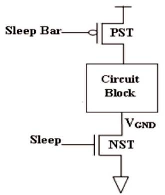
Figure 1. Sleep Approach
For retaining data during idle periods, a significant voltage across the blocks must be maintained. Clamping devices like MOSFETs and diodes, in addition to sleep transistors are used for this purpose. All the techniques discussed in this paper offer data retention except sleep approach.
Dual diode Vth approach shown in Figure 2 reduces the overall power consumption significantly, by maintaining a conventional sleep mode and an intermediate drowsy mode. Dual diode Vth approach (Kumagai et al. 1998) adds a series combination of NMOS or PMOS (PDT or NDT) and a diode in parallel with the sleep transistors (PST and NST). In the drowsy mode, PST and NST are turned off and PDT and NDT are turned on. The diodes in series with the MOS transistors help to reduce leakage significantly along with data retention realization. Ground bounce also gets decreased in this approach at increased area overhead.
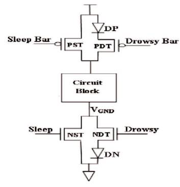
Figure 2. Dual Diode Vth (DDV) Approach
Dual switch approach shown in Figure 3 employ transistors NDT and PDT in parallel with the conventional sleep transistors (NST and PST) (Chowdhury et al. 2008). A low leakage drowsy mode is realized by turning on NDT and PDT while PST and NST are turned off. In the drowsy mode, leakage power consumption is minimized while the data is preserved by maintaining a reduced yet significant voltage difference between the virtual lines. Area overhead is high in this technique as compared to the sleep approach.
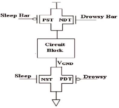
Figure 3. Dual Switch (DS) Approach
Kim et al. (2007) proposed a power gating structure which supports the traditional sleep mode and drowsy mode. This approach is shown in Figure 4 and it utilizes a transistor DT in parallel with sleep transistor (NST). By applying zero gate voltage to NST and DT, the circuit can be put in the intermediate power saving mode whereby power reduction and data retention are both realized. In this approach, the virtual ground voltage is limited by the threshold voltage of the transistor DT, hence it is not possible to vary the virtual ground voltage over a range of values.
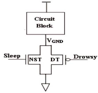
Figure 4. Trimode Power Gating (TPG) Approach
The three transistor approach ( Jiao and Kursun, 2011) is shown in Figure 5. A drowsy transistor DT is used in parallel with sleep transistor. In the sleep mode, the power supply to the circuit block is disrupted, by making the two sleep transistors (PST and NST) and the Drowsy Transistor (DT) off. In the drowsy mode, the two sleep transistors are turned off while the drowsy transistor is maintained on. The virtual ground voltage is raised by the threshold voltage of the drowsy transistor, for maintaining a voltage difference across the circuit block which is necessary for data retention. This technique suppresses the ground bouncing noise while implementing a data retention drowsy mode.
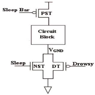
Figure 5. Three Transistor Controlled (TTC) Approach
In dual-diode Vth, dual switch, trimode and three transistor controlled approaches, when the circuit is in active mode, charge is stored at the gate of the sleep transistor and it is abandoned to ground as the circuit moves to sleep state. No attempt is made to use the charge at the gate of the sleep transistor. Sleep buffer, trimodal switch and pass transistor techniques which are discussed below reuse the charge stored at the gate of sleep transistor and reduce leakage.
Tada et al. (2006) proposed the sleep buffer approach shown in Figure 6, which controls the degree of drowsiness of the circuit by using a negative feedback, through the sleep buffer. The virtual ground voltage is boosted by reusing the charge at the gate of the sleep transistor through the transistor MS2. This approach clamps the voltage level of the virtual ground node using negative feedback without using any clamp devices. This approach reduces leakage current through sleep control circuits as well as internal circuits. This technique works fine for small standby periods when the circuit switches back and forth between drowsy and active modes frequently but it fails to be effective for long idle periods due to large amount of leakage.
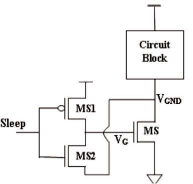
Figure 6. Sleep Buffer (SB) Approach
Tri modal switch approach shown in Figure 7 was suggested by Pakbaznia and Pedram (2012). When sleep signal is low, MS1 is on and the voltage level at VG is VDD . Thus independent of the value of the drowsy input, the MS transistor is on and the circuit is in the active mode. When sleep signal is high, the trimodal switch operates in the sleep or drowsy mode depending on the value of the drowsy signal. In particular, if drowsy signal is low, transistors MS2 and MD2 are on, MS is off and the tri-modal switch cell operates in sleep mode. If both sleep and drowsy signals are high, MS2 and MD1 are on creating a negative feedback between VGND and VG nodes, which puts the circuit block into drowsy mode. In sleep mode, there exists a sneak path from VDD to the ground through MS1, MS2, and MD2.
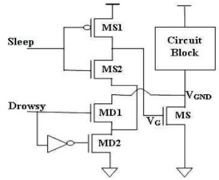
Figure 7. Tri Modal Switch (TMS) Approach
Pass transistor approach ( Liu and Kursun, 2007) is illustrated in Figure 8. In this approach, the virtual ground line is connected to the sleep signal line through a Pass Transistor (PT). In the active and sleep modes, the pass transistor is turned off. Pass transistor is on in drowsy mode and the charge stored at the sleep signal line is recycled through the pass transistor during mode transitions. The charge recycling process continues until the voltages of the virtual ground rail and sleep signal line are equalized and thus the virtual ground node voltage has been raised for providing data retention.
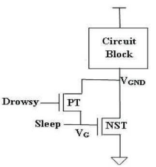
Figure 8. Pass Transistor (PT) Approach
For analyzing the performance of the power gating techniques discussed in this paper, current and power consumption in sleep and drowsy mode are estimated. Synopsys HSPICE is used for simulation of two input NAND gates using 90 nm PTM technology ( Zhao and Cao, 2006). For estimating leakage current and power, the circuit blocks are maintained in sleep mode. As leakage depends on the inputs given, all possible input combinations are applied and the resulting power is averaged and tabulated in Table 1. For drowsy power estimation, circuit block is made to switch from active to drowsy mode and the results are also averaged and listed in Table 1. Current and power comparisons of various gating techniques are also shown in Figures 9 and 10.
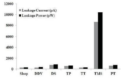
Figure 9. Leakage Current and Power Comparison
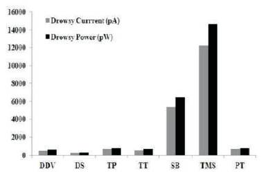
Figure 10. Drowsy Current and Power Comparison
From Table 1, it is evident that sleep approach provides low leakage compared to other techniques but it suffers from data loss during idle periods due to the absence of drowsy mode. Dual-diode Vth and dual switch techniques offers low leakage and drowsy power, however the area overhead is high in these techniques. Trimode and three transistor techniques power gating presents a good leakage and data retention capability but the virtual ground (VGND ) voltage is limited by the threshold voltage of the MOS devices and hence it is not possible to vary VGND voltage. Virtual ground voltage can be varied in sleep buffer, trimodal switch and pass transistor approaches. From the simulation results shown in Table 1, it is clear that sleep buffer technique is not suitable for long idle periods due to the absence of sleep mode. Trimodal switch approach experiences high power consumption as well as more area overhead. Leakage and drowsy power of pass transistor approach is low only if the pass transistor is sized properly.
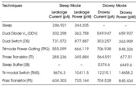
Table 1. Current and Power Analysis of Various Power Gating Techniques
Excessive power consumption is a major hindrance to the advancement of nanoscale CMOS VLSI circuits. Suppressing sub threshold leakage currents and designing low power VLSI circuits is essential to achieve green computing and to extend battery lifetime of portable and self-sustaining applications. This survey paper briefs about the different power gating techniques intended for static and dynamic power minimization. All power gating techniques discussed in this paper have their own advantages and limitations. Power gating techniques with low leakage suffer from data loss in standby periods whereas power gating with data retention capability experience high area overhead. Power gating structures with improved performance is necessary to meet the stringent power requirements of mobile devices.