In modern CMOS technology, the growing demand of low cost integrated circuit requires RFICs featuring low power consumption, high level integration and high data rates, have become critical in wireless systems at around 10 GHz for emerging applications. By employing silicon-based technology it is possible to design low cost direct conversion receivers targeted at 8 - 40 GHz frequency bands. The main focus is on the design and implementation of a receiver front-end for Ka - band (27 - 40 GHz) applications. The drawbacks of these designs are LO self-mixing and 1/f noise. To overcome these drawbacks, a dual - band receiver is proposed to be designed by adopting a wideband two stage LNA and wideband mixer in a 0.18 μm Bipolar Technology. To suppress the LO self-mixing problems, the sub harmonic mixer is applied to the receiver and by adopting a 3D inductor, IF 3-dB bandwidth can be improved. The designs are modeled in SPICE and verified in HSPICE Synopsys tools.
Low Noise Amplifier (LNA) is an electronic device which amplifies a very low power signal without significantly diminishing its signal to noise ratio. An amplifier increases the power of both the signal and the noise present at its input. Low Noise Amplifiers are designed to reduce the additional noise. Designers minimize the additional noise by considering tradeoffs like impedance matching. Choosing the amplifier technology, we can select low noise biasing conditions. Low Noise Amplifiers are found in radio communication systems, medical instruments, and electronic equipment. A typical Low Noise Amplifier may supply a power gain of 100 (20 dB) while decreasing the signal to noise ratios by less than a factor of two (a 3 dB noise figure). Although low noise amplifiers are primarily concerned with weak signals which are just above the noise floor, they should also consider the presence of larger signals that causes inter modulation distortion. Consequently, a low noise amplifier often does not have high gains. Feedback techniques can be used in circuits, which the poles of active devices are in frequencies well above the feedback loop bandwidth. With an increasing cut-off frequency (fT) of MOS transistors in recent years, it has been made possible to use feedback in high frequency LNA circuits. Feedback loop is useful in wideband matching of CS stages. In resistive feedback has been used in design of cascade multi band LNA for multi standard transceivers. In RLC, feedback has been used in wideband matching of a cascade stage. Feedback techniques are often used in designing low noise amplifiers in order to shift the optimum noise impedance to the desired point. Feedback reduces the non-linearity of the circuit and improves IIP3 point. General considerations to design Low Noise Amplifier are noise performance, power transfer, impedance matching, power consumption, bandwidth, stability and linearity. The Sub-Harmonic Mixer (SHM) topology is adopted for avoiding the LO self mixing problems [1], [3] and its low DC offset attributed to the local frequency is half of the RF frequency. In this study, the switching pairs of the mixer core circuit are implemented with the Bipolar-Junction-Transistor (BJT). The BJT device exhibits a lower 1/f noise corner below 10 KHz [5]. The needed input power level of the local oscillator can be reduced by about 6 dB compared to the MOS transistor switching cores. A 24-GHz receiver front-end using multistage LNA successfully enhanced the gain and the noise performance by the source denegation inductor. However, such design requires a considerable amount of inductors, resulting in a large chip area [4]. A dual-band receiver was designed by adopting a wideband two-stage LNA as well as a wideband mixer in a 0.18-μm BiCMOS technology [2], [6], [7].
The main focus is on the design and implementation of a receiver front-end for Ka – band (27 - 40 GHz) applications. The drawback of these designs are LO self-mixing and 1/f noise. To overcome these drawbacks, a dual – band receiver is proposed to be designed by adopting a wideband two stage LNA and wideband mixer in a 0.18μm Bipolar Technology.
Narrow band Low Noise Amplifiers typically uses LC tuned and integrated inductors. Because of using LC tuned and integrated inductors, the area and cost increases. To overcome these drawbacks, wideband low noise amplifiers are used. The advantages of wideband low noise amplifiers are more bandwidth, frequency resolution is low, sensitivity is poor, dynamic range is fair, speed of acquisition is high, power requirement is low, immunity to jamming is poor, cost is low, high data rates and high throughput.
A well-designed LNA is critical to the overall system performance, which in this design should provide wideband power and noise matching. A straightforward approach is to adopt the common-gate topology. Typically, the single- ended Zo is 50 Ω, and therefore a GM of 20 ms is required. However, such constraint limits the DC bias current and the aspect ratio of the input transistor. This problem is solved by taking advantage of the impedance transform techniques in this study. The topology of the LNA circuit is shown in Figure 2, which is similar to the authors’ previous design [8]. The two-stage LNA circuit is designed aiming for low NF and wideband input matching, also with the power gain to be up to 20 dB. The GM boost stage is composed of M1-2 and CC to amplify the small signal input as well as suppress the internal noise contributed by the mixer and the IF amplifier. The M3-6 form the second stage of cascode amplifier to further enhance the overall power gain. Compared to the typical Common-Source (CS) amplifier, the cascode topology provides advantages such as better gain performance, improved stability, and enhanced reverse isolation [9]-[12]. The two-stage LNA only consumes 12 mA under a 2V supply voltage in final design.
In order to realize the input impedance transformation, the circuit which is shown in Figure 1 is modified.
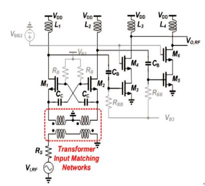
Figure 1. Two Stage LNA using Transformer Inductors
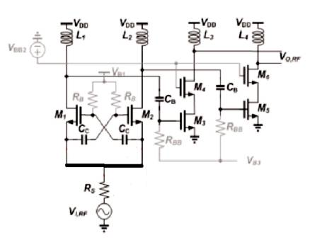
Figure 2. LNA using CMOS Technology
The circuit of LNA using CMOS technology is simulated in HSPICE_A 2008 .03. Figure 3 shows the simulated result of LNA using CMOS technology.
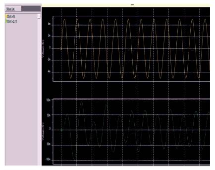
Figure 3. Simulated Result of LNA using CMOS
The following are the parameters obtained after simulation. Using Awanwaves, the output waveforms are seen. Using HSPICERF, the Total Noise and Noise Figure can be seen. Simulated CMOS Technology based LNA parameters are tabulated in Table 1. The Gain is increased by 10 times when compared to the Bipolar Technology based LNA. The Gain achieved by using Bipolar Technology based LNA is 2 dB and for CMOS Technology based LNA is 20 dB.
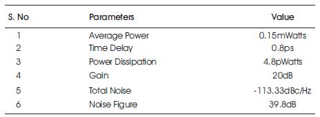
Table 1. Simulation Results of LNA using CMOS Technology
This work successfully demonstrated a wideband receiver front-end in a low cost 0.18 μm SiGe CMOS technology. The proposed receiver front-end takes the advantages of less delay and good noise figure. By employing silicon-based technology, it is possible to design low cost direct conversion receivers that gives low power consumption, high level integration and high data rates. Different parameters like Average Power, Gain, Time Delay, Total Noise, Noise Figure and Power Dissipation for CMOS technology are calculated. By using CMOS technology, the gain is increased. The Gain for LNA using CMOS Technology is 20 dB with Total Noise is -113.33 dBc/Hz and with Noise Figure is 39.8 dB. The average power is 0.15 mWatts with time delay 0.8 psec for two stage LNA using CMOS technology.