 |
i-manager's Journal on Future Engineering and Technology |
View PDF |
|||
| Volume :11 | No :2 | Issue :-2016 | Pages :25-36 | ||
In the present scenario, Nanophysics and Nanochemistry are relatively new areas of science arisen in the last decade after the discovery of fullerenes and nanotubes. Nano sized materials are used in numerous applications ranging from electric storage device, science and engineering, which will bring a wave of radical innovation . It has a potential broad impact, spark in various application areas such as: drug delivery to treat tumour, cancer (without using radiotherapy & chemotherapy), solar energy, batteries, display technologies, Opto- electronic devices, semiconductor devices in nanoelectronics, biosensors, CNT's etc. The expectations on nanomaterials are enormous as their unique Mechanical, Optical, Electrical, Magnetic, Thermal and Catalytical properties make them special ingredients for a number of applications. This paper describes introduction to the most interdisciplinary integrated modern science known as nanotechnology. Classification and properties of nanomaterials, synthesis of Nanomaterial, and its growth, significance, applications in various fields. The new material terminologies associated with this field. This paper gives a short overview of some of the different types of nanomaterials such as graphite, fullerenes and carbon nanotube, etc.
Nanotechnology is a fundamental multidisciplinary science that has roots in almost all the fields of Science and Technology. It deals with design and production of objects or structure at a very small scale and on the level of nanometers (one-billionth of a meter). It is the extension of existing science into nano scale. In the metric system of measurement, "Nano" means 10-9 and therefore a nanometer is one-billionth of a meter. Richard P. Feynman, a noble laureate in Physics brought this nanotechnology into daylight in the year 1959 and inspiration to many researchers in the world [1,2].
Nanoscience is the study of fundamental principles of molecules and structures having sizes between 1 and 100 nm, these are known as nanostructures. Nanomaterials are cornerstones of nanoscience and nanotechnology. In the present scenario, Nanostructure science and technology is a broad and exciting area of research and development activity that has been growing explosively worldwide in the past few years. It has the potential for revolutionizing the ways or methods in which, the materials and products are created. It is having a most significant commercial impact, which will be assuredly increased in the future. At present, Nanotechnology for sustainable energy production is one of the fastest growing research fields in the world and it leads to the development of a renewable energy economy [3]. When it comes to application and development, many of the proven technologies based on nanomaterials are related to many products such as, water filters, medical textiles, cosmetics and drug delivery, etc.
Recently in April 2010, US EPA has announced a new definition on nanomaterials as "an ingredient that contains particles that have been intentionally produced to have at least one dimension that measures between approximately 1 and 100 nanometers" in order to facilitate the implementation of regulations on use of nanomaterials in commercial product [4].
Further macroscopic composite materials, which contain objects at the nanoscale, have been deliberately engineered to create novel properties [5]. Examples of this kind of material are: carbon nanotubes introduced in a polymer matrix to make it conductive, nanocomposite steel alloys which are engineered to withstand extremely high loads, and other everyday products such as rubber containing carbon black (for car tyres), integrated electronic circuits example of this kind is MEMS (Micro- Electro-Mechanical Systems) and electronic displays today may include features in the nanoscale regime in a much more structured way [4, 5]. Such composite and electronics products, as well as other materials like nanoporous materials, are also considered as nanomaterials, due to the nanostructures which are incorporated in order to modify their properties.
Nanomaterials have different Physical and Chemical properties to those of bulk materials. Some of these properties can be extrapolated from the macroscale (Ex: In some cases, materials that are inert in their larger form are reactive when they produce in their nanoscale form). In some cases, others change their characteristics drastically at a certain size (true nanoscale features). Although a material may not necessarily show true nanoscale features, it can have properties that are clearly different from those of the bulk just because of its reduced size. Therefore, a definition for nanomaterials must encompass both properties deriving from pure downscaling and true nanoscale features. Because, there is no unique relationship between size and physical, chemical properties which is valid for all the materials, the only feature common to all nanomaterials is the nanoscale [6].
Non-scalable properties on the other hand exhibit unique nanoscale features below a certain size. Examples include confinement effects such as, the increased band gap of semiconductor nanoparticles - quantum dots - such as lead selenide (PbSe), cadmium selenide (CdSe) and cadmium sulphide (CdS), which increases dramatically for diameters below 5 nm, or thermal properties such as the melting point of indium and tin nanoparticles decreases exponentially below a diameter of 15 nm.
According to a recent study by a market researcher, the annual worldwide market for products incorporating nanotechnology is expected to reach US $3.3 trillion by 2018. According to the National Nanotechnology Infrastructure Network, the need for technology professionals working in nanotechnology will increase to 1 million employees by 2015.
Nanotechnology is the new word for chemistry, it is a great term for creating public interest and for collaborative research, where we can now do things more efficiently and with higher performance by making use of nanoscale scientific principles. This technology has enabled advances in computer memory, storage capacity, reduced power consumption, and increased speed, Semiconductors applications everything else combined in this.
At present, the number of labs working with nanomaterials is growing dramatically and they are looking for all kinds of new nano properties, for applications ranging from catalysts to energy conversion to deal with issues such as cleanliness and nanofabrication quality control.
Nanomaterials are materials which have extremely small size, characterised by an ultra fine grain size (<50nm) have at least one dimension 100 nm or less (dimensionality limited to 50 nm).
For comparison, a red blood cell is approximately 7000 nm wide and water molecule is almost 0.3 nm across. Figure 1 shows the relationship between bulk material and nanomaterial. These materials have created a high interest in recent years by virtue of their unusual mechanical, electrical, optical and magnetic properties. Nanosized materials are used in numerous applications ranging from electric storage device, science and engineering which will bring innovation and perhaps, because of its potential these are used in various application areas.
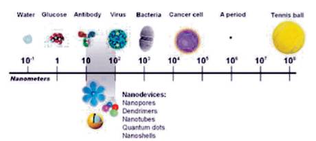
Figure 1. Image Adopted from "A Snapshot of Nanotechnology" National Cancer Institute
There are various approaches for classification of nanomaterials. Nanoparticles are classified based on one, two and three dimensions (Hell 2004) [7]. According to Richard W. Siegel, nanomaterials are Zero (atomic clusters, filaments and cluster assemblies), one dimension (thin films and surface coating), two dimension (ultrafine grained over layers or buried layers) and three dimension (nanomaterials consisting of equiaxed nanometer sized grains) [8, 9].
Nanomaterials have one dimension less than 100 nm (Ex: thin films and surface coatings). Nano objects have two dimensions less than 100 nm (Ex: Carbon nanotubes). Nanoparticles are defined as particles with three dimensions of less than 100nm. One-dimensional nanomaterials, such as thin films, layers and surfaces, have been developed and used for decades in the fields such as, Electronic device manufacture, chemistry and Engineering. Common types of nanomaterials include nanotubes, quantum dots, dendrimers and fullurenes.
Figure 2 shows the classification of nanomaterials. Nanomaterials (eg. gold, carbon, metals, meta oxides and alloys) with variety of morphologies (shapes) are shown in Figure 3.
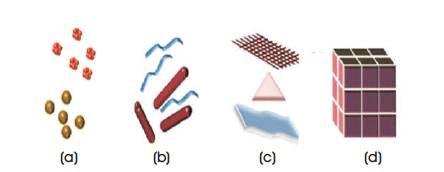
Figure 2. Classification of Nanomaterials: (a) 0D Spheres and Clusters, (b) 1D Nanofibers, Wires and Rods, (c) 2D Films, Plates and Networks (d) 3D Nanomaterials [ 7]
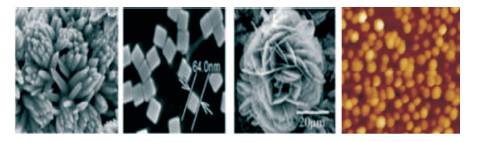
Figure 3. Nanomaterials with Variety of Morphology (Titanium Nanoflower, Silver Nanocubes, SnO2 Nanoflower, Au Nanoparticles) [7]
Nanomaterials are designed at the molecular (nanometre) level to take advantage of their small size and novel properties which are not seen in their conventional, bulk counterparts. The bulk properties of materials often change dramatically with nano ingredients. Composites made from particles of nanosize ceramics or metals smaller than 100 nm can suddenly become much stronger than predicted by the existing materials [10] (Ex. Metals with so called grain size of around 10 nm are as much, as they are seven times harder, stronger and tougher than their ordinary counterparts).
In addition to geometric properties like size, surface area and shape, a nanomaterial can be characterised by its physical-chemical properties, as any other material. It may become crucial if an upper size limit (Ex: 100 nm) specified in the nanoscale definition would be too restrictive to capture all the materials that exhibit specific properties due to their structure in the nanoscale. Very small size form of matter such as atoms and molecules have their own set of rules and don't behave the same way as larger objects. Figure 4 shows the nanoworld in which, Nanomaterial properties can change with size [11].
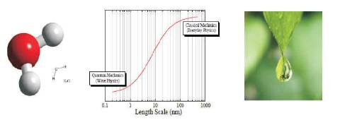
Figure 4. Nanoparticle Change with Size
The properties of material can be different at the nanoscale due to two main reasons. The two main reasons why materials at the nano scale can have different properties are increased relative surface area (nonmaterials have relatively larger surface area when compared to the same mass of material produced in a larger form) and new quantum effects (dominate the behaviour of matter at the nanoscale).
Nanomaterials have a relatively larger surface area when compared to the same volume or mass of the material produced in a larger form. When a bulk material is reduced to the particles of smaller size, then the surface area to volume ratio becomes very high. For example, for a spherical material of radius r, the surface area is given by,
Surface area = 4πr2
And its, volume = 4/3πr3
Surface area to volume ratio is =4πr2/4/3πr3 =3/r
For nanospherical material, due to decrease in size (r), the above ratio increases predominantly [12].
So the particle size decreases, a greater proportion of atoms are found at the surface compared to those inside. Hence, nanoparticles have a much greater surface area per given volume compared with larger particles. This makes the material more chemically reactive and affects their strength or electrical properties. Figure 5 shows the increased surface area results from dividing the larger particle into many smaller pieces. Surface Area is a big factor implies that, mass and volume of the material is unchanged by the division of the block into small pieces.
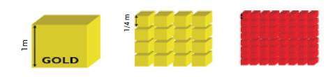
Figure 5. Larger Material is divided into Many Smaller pieces
Quantum confinement effect is observed when the size of the particle is too small to be comparable to the wavelength of the electron. The word confinement means to confine the motion of randomly moving electron to restrict its motion in specific energy level. In nanocrystals, the electronic energy levels are not continuous as in the bulk, but are discrete (finite density of states); because, of the confinement of the electronic wave function to the physical dimensions of the particles.
This phenomenon is called as “Quantum confinement” [13, 14]. At the nano scale, quantum effects can become much more important in determining the materials properties and characteristics, leading to novel optical, electrical and magnetic behaviours. If one length of three dimensional nanostructures is at nano-dimension, then it is called as “Quantum Well”. If two sides of three dimensional nanostructures are at nano-dimension, then it is called a “Quantum Wire”. If all the three dimensional nanostructures are at nano-dimension (Nano Crystals), they are referred as “Quantum Dots (QDs)”. If the size of quntum dot is smaller than that of Bohr radius, then confinement occurs leading to a transition from continuous to discrete energy levels.
Nanomaterials have properties that are different from those of bulk materials [15,16]. Most nanostructure materials are crystalline in nature and they have unique properties that lead to significant improvements in their mechanical properties. Recently, many scientists have developed their efforts to study the physical properties of metallic nanoparticles and ultra thin films, expecting to obtain a right perspective to the essential features of quantum confinement. Many exotic physical properties have seen with quantum size effect such as, the splitting of the continuous conduction band into discrete levels, the electromagnetic field enhancement on the surface, the magnetic properties changes from diamagnetic into paramagnetic, and from ferromagnetic into super paramagnetic. Nanomaterials and Nanotechnologies attract tremendous attention in recent scenario. New physical properties and new technologies both in sample preparation and device fabrication evoke on account of the development of nanoscience [17].
Crystal structure of nanoparticles is same as the bulk structure with different lattice parameters. The interatomic spacing decreases with size and this is due to long range electrostatic forces and the short range core-core repulsion. As a result, the melting point of nanoparticles decreases with size [12].
A large fraction of the atoms are located at the surface of the nanomaterial, which increase its reactivity and catalytic activity. The large surface area to volume ratio, the variations in geometry and the electronic structure of nanoparticles have a strong effect on catalytic properties.
The mechanical behaviour of nanoparticles is due to the nature of interfaces in them. Mechanical properties such as hardness, toughness, elastic modulus, scratch resistance, fatigue strength and crack initiation and propagation are significantly different for nanostructures than bulk material. For example in metals and alloys, the hardness and toughness increases by reducing the size of nanoparticles. In ceramics, ductility and super plasticity are increased on reducing the particle size. Fe and Ni continue to harden with decreasing grain size. By decreasing the size of nanocrystalline metals from 1μm to 10 nm and the hardness increases by 2 to 7 times. As the grain size is reduced below 10 nm the hardness reduces in some nanomaterials. At higher temperatures, some nanoparticles possess superplastic property. When the material is superplastic, it can undergo large tensile deformation without getting cracks [13].
The energy band structure and charge carrier density in the materials can be modified quite differently from the bulk material and in turn that will modify the electronic properties of the materials. Nanoparticles made of semiconducting materials like Germanium, Silicon and Cadmium are not semiconductors. Further, nanoclusters of different sizes will have different electronic structures and different energy level separations. So they show diverse electronic properties which depend on its size.
The magnetic moment of nano particles is found to be very less when compared with its bulk size. Actually, it should be possible that non-ferromagnetic bulk exhibit ferromagnetic-like behaviour when prepared in nano range. Bulk Gold and Platinum are non-magnetic, but at the nano size, they are magnetic [18,19]. One of the fascinating properties of magnetic nanoparticles is the reduction from multidomains to a single domain as the particle size reduces to some limit values. At high temperatures, single domain magnetic nanoparticles are thermally free to orient their spin directions and exhibit super paramagnetic properties. The super paramagnetic state is blocked as temperature lowers down to enhance the exchange interactions between particles.
The optical emission and adsorption occurs when the transition of the electrons occur between these two states. Semiconductors and many metals show drastic changes in optical properties such as color, as a function of particle size. Colloidal suspenses of gold nano particles have a deep red color, which becomes progressively more yellow as the particle size increases.
The most significant challenge in the research and development of nanoparticle is the synthesis and characterisation of various novel materials with well controlled size, shapes, porosity, crystalline phases, and structure and must be inexpensive. Figure 6 shows the various facts that should be controlled in the synthesis of nanomaterials [20].
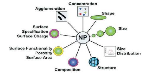
Figure 6. Some of the Key Parameters to Characterize the Synthesis of Nanomateerials [35]
There are many methods for the production of nanomaterials. Few well known methods are sol-gel synthesis, mechanical alloying or high energy ball milling, plasma synthesis, Electrode position, colloidal suspension, chemical vapour deposition, inert gas condensation etc [21]. Among these methods, some techniques are explained ion the following sections.
Sol-gel technology is a very popular and well established colloidal technology; it offers possibility of producing various materials with novel, predefined properties in a sample process and at relatively low process cost.
In sol–gel method, a colloidal solution is used for the preparation of nanomaterials. The sol is a name of colloidal solution made of solid molecules or particles (having diameter in the range of 20 nm to 100 nm) suspended in liquid phase. The formation of inorganic networks with colloidal suspension in a continuous liquid phase is called gel. The gel can be considered as a solid macromolecule immersed in a solvent.
The typical precursors used for synthesizing these colloids are usually a metal or metalloids element surrounded by various reactive ligands. In this method, the starting material is processed to form a dispersible oxide and forms a sol in contact with water or dilute acid. Removal of the liquid from the sol yields the formation of gel, and the sol/gel transition controls the particle size and shape. Calcination of the gel produces the oxide.
Sol-gel processing refers to the hydrolysis and condensation of alkoxide-based precursors such as Si (OEt) 4 (tetraethyl orthosilicate, or TEOS). The reactions involved in the sol-gel chemistry based on the hydrolysis and condensation of metal alkoxides are given below.
M (OR)z can be described as follows:
MOR + H2O → MOH + ROH (hydrolysis)
MOH + ROM →M-O-M + ROH (condensation)
The sol gel process can be explained in the following steps.
This process is complicated due to fundamental changes in the structure of the gel. The drying process has itself been broken into four distinct steps:
If isolated by thermal evaporation, the resulting monolith is termed a xerogel. If the solvent (such as water) is extracted under supercritical or near super critical conditions, the product is an aerogel.
Densification and decomposition of the gels at high temperatures (T>8000o C). The pores of the gel network are collapsed, and remaining organic species are volatilized. The typical steps that are involved in sol-gel processing are shown in the schematic diagram below. Figure 7 shows the schematic representation of sol-gel process.
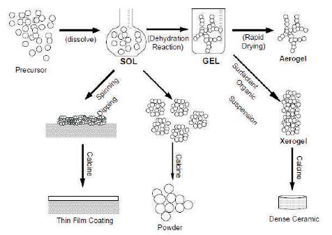
Figure 7. Schematic Representation of Sol-gel Process of Synthesis of Nanomaterials [7]
Sol-gel method is a long established industrial process for generating colloidal nanoparticles from liquid phase. It has been further developed in the last years for the production of advanced nanomaterials and coatings. Sol-gel techniques show many advantages like low temperatures during processing, versatility and easy shaping and embedding. Common precursors which are used for the production of oxides are alkoxides, due to their availability and to the high liability of the M-OR bond allowing facile tailoring during processing. The main benefits of sol gel processing are the high purity and uniform nanostructure achievable at low temperature [19, 22].
This technique is a widely used in materials-processing technology due to its low set-up cost, high production yield, and ease of scale-up [20].
Chemical Vapor Deposition (CVD) is referred to as the activating chemical reactions between a substrate surface and a gaseous state.
Precursor in order to a thin solid film is deposited onto the substrate [23]. Activation can be achieved either with increased temperatures (Thermal CVD) or with plasma (PECVD: Plasma Enhanced Chemical Vapour Deposition); decreasing significantly the process temperature compared to the thermal CVD process. Chemical vapor deposition has been developed as a novel manufacturing process in many industrial sectors such as, semiconductor and ceramic industry [24].
Chemical Vapor Deposition method is used to prepare nanoparticle of composites BaTiO3 , metal oxides, metal carbides etc. Chemical vapour deposition method consists of three important parts namely i) heating chamber ii) reaction chamber iii) cooling chamber. The method of getting nanoparticles is explained in the following sections.
A metal organic precursor is taken into the heating chamber and is heated to high temperature; so that, it can be melted and evaporated. The gases are delivered into a reaction chamber operated at a suitably determined high temperature (500–1200o C). Also, inert gases, such as argon and nitrogen, are usually used as carrier gases. The gases pass through the reactor coming into contact with the heated substrate; undergo condensation through nucleation and form clusters. The reaction products or clusters from the reaction chamber are passed into the cooling chamber. Liquid nitrogen is used for cooling this chamber.
This cooling chamber contains a rotating cylindrical device on a cold finger. A scraper is attached to the rotating device. The nanoparticles are allowed to condense on the rotating cylindrical device and scrapper is used in collecting the nanoparticles. Figure 8 shows the schematic representation of CVD technique [13].
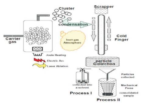
Figure 8. Schematic Representation of CVD System [7]
In the present scenario, CVD is the promising method for scaling-up compared to arc discharge and laser assisted methods. Recently, a Swirled Floating Catalytic Chemical Vapour Deposition (SFCCVD) reactor was developed for enhancing the production capacity using a vertical reactor inside a furnace and cyclones for collecting the final product. Chemical and physical vapor deposition can be used for the growth of semiconductor nanotubes, including ordered arrays of CNTs. CVD process also takes place in a three-zone furnace with deposition temperatures varies from 500 to 1000oC. CVD techniques, particularly plasma assisted CVD, show many perspectives to grow aligned nanotubes of complex semiconductor or oxides.
CVD is a vital process used to produce thin coatings of high purity. The deposition of the thin films can be performed at considerably lower temperature by applying different types of catalysts. Recently Catalyst Enhanced Chemical Vapor Deposition (CECVD) has emerged as a new enhancement technique. It is particularly suitable for the deposition of metallic films on thermally sensitive substrates [25].
Synthesis of nanomaterials by a simple, low cost and in high yield has been a great challenge in the development of nanomaterials. There are various techniques in bottom up and top down approaches for the commercial production of nanomaterials. The different type of ball milling can be used for synthesis of nanomaterials in which, balls impact upon the powder charge [26]. The typical mill used for these purposes are the high energy ball mill such as, tumbler ball mills, vibratory mills, planetary mills, and attritor mills (Szegvari attritor), etc. Among all top down approaches, high energy ball milling has been widely used for the synthesis of various nanomaterials.
In this method, a suitable powder (typically, a blend of elemental) is placed in a high energy mill, along with a suitable milling medium. The objective of milling is to reduce the particle size and blending of particles in new phases. The balls may roll down in the chamber in a series of parallel layers. For large scale production with nano size grain, mechanical millings are more economical processes [27].
Mechanical milling is typically achieved using high energy planetary ball, or tumbler mills. The energy transferred to the powder from refractory or steel balls depends on the rotational (vibrational) speed, size and number of the balls, ratio of the ball to powder mass, the time of milling and the milling atmosphere. Mechanical attrition is a typical example of 'top down' method of synthesis of nanomaterials, where the material is prepared not by cluster assembly, but it is by the structural decomposition of grained structures as the result of severe plastic deformation. This has become a popular method to make nanocrystalline materials because of its simplicity, the relatively inexpensive equipment. The major advantage of this method is the possibility for scaling up the quantities of material for various applications.
Ball mill is a cylindrical drum containing grinding ball inside the drum and it is used in grinding the material. The balls are usually made up of dense materials like steel or tungsten carbide. The system is particularly suitable for research purpose in the laboratory. The ball mill system consists of one turn disc (turn table) and two or four bowls. The turn disc rotates in one direction, while the bowls rotate in the opposite direction. The centrifugal forces, created by the rotation of the bowl around its own axis together with the rotation of the turn disc, are applied to the powder mixture and milling balls in the bowl. The powder mixture is fractured and cold welded under high energy impact. Since the rotation directions of the bowl and turn disc are opposite, the centrifugal forces are alternately synchronized. Thus friction resulted from the hardened milling balls and the powder mixture being ground alternately rolling on the inner wall of the bowl and striking the opposite wall. The impact energy of the milling balls in the normal direction attains a value of up to 40 times higher than that due to gravitational acceleration. Hence, the planetary ball mill can be used for high-speed milling. This method is used for preparing nano particles for a large number of elements and metal oxides [13]. Figure 9 shows the schematic representation of ball mill technique.
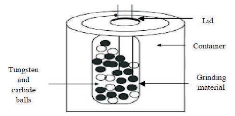
Figure 9. Schematic Representation of Ball Mill Technique
There are many new material terminologies associated with this field. This section gives a short overview of some of the different types of nanomaterials.
Nanomaterials offer interesting physicochemical and biological properties for biomedical applications due to their small size, large surface area and ability to interact with the cells or tissues. Graphene-based nanomaterials are fast emerging as "two-dimensional wonder materials" due to their unique structure and excellent mechanical, optical and electrical properties and have been exploited in electronics and other fields. Emerging trends show that, their exceptional properties can be exploited for biomedical applications, especially in drug delivery and tissue engineering.
Graphene is a one atom thick planar sheet of carbon atoms densely packed in a honeycomb crystal lattice [28]. Graphene is the basic structural building block of carbon nanotubes and fullerenes. Carbon nanotubes (CNT) also known as 'buckytubes' have a cylindrical nanostructure in the form of a tube and an engineered CNT typically has a nanoscale thick wall, geometrically shaped similar to a Buckyball, with a nanoscale diameter, and a length that may exceed 100 nm. Graphene is undoubtedly emerging as one of the most promising nanomaterials because of its unique combination of superb properties, which opens a way for its exploitation in a wide spectrum of applications ranging from electronics to optics, sensors, and biodevices etc.
Because of high quality sheets of graphene, it is often prepared by Chemical Vapor Deposition (CVD), which requires an expensive equipment. Many researchers have looked at using graphene oxide as a solution processable alternative for the preparation of grapheme like materials. Indeed, graphene oxide can be reduced in solution and as a thin film using a variety of reducing conditions that has a large enhancement in electrical conductivity [29, 30]. Graphene oxide has been used in catalytic oxidation, biotechnology, and as a surfactant. Graphene-based nanomaterials have many promising applications in energy-related areas. Just some recent examples: Graphene improves both energy capacity and charge rate in rechargeable batteries; activated graphene makes superior supercapacitors for energy storage; graphene electrodes may lead to a promising approach for making solar cells that are inexpensive, lightweight and flexible; and multifunctional graphene mats are promising substrates for catalytic systems.
Carbon nanotubes are manufactured as Single Wall Carbon Nanotubes (SWCNT) or Multiwall Carbon Nanotubes (MWCNT) [31, 32]. They are synthesized in a variety of ways, including arc discharge, laser ablation and chemical vapor deposition. With respect to tensile strength, carbon nanotubes are the strongest and stiffest materials yet discovered. Since CNTs have a very low density, their specific strength is 300 times greater than stainless steel, though under compression CNTs appear to be a lot weaker. Carbon nanotube is one of the most promising materials in recently developed materials on account of its superior properties of rigidity, strength, elasticity, electric conductivity, and field emission.
Most existing substrates for growth of carbon nanotubes (CNTs) by Chemical Vapor Deposition (CVD) process are silicon wafers deposited on a thin film of transition metal catalysts on which carbons are dissolved and precipitated in hexagonally packed graphite on the cooling surface side [33].
Quantum dots, also known as nanocrystals, are another form of nanomaterial and are a specific type of semiconductor [34]. They are 2-10 nanometers (10-50 atoms) in diameter, and because of their electrical characteristics, they are [electrically] tunable. The electrical conductivity of semiconductors can change due to external stimulus such as voltage or exposure to light, etc. Quantum dots are typically made from the compounds like CdSe, ZnS or CdTe though a EU Restriction of Hazardous Substances (RoHS) perspective, cadmiumfree quantum dots are required.
Fullerene is any molecule in the form of a hollow sphere, ellipsoid or tubular structure composed entirely of carbon. They are commonly referred to as "Buckyballs" – named after Buckminster Fuller who designed geodesic physical structures and buildings based on this geometry. A Buckyball is a carbon based hollow geometric sphere, first found in soot developed from a laboratory experiment [35]. It resembles a hollow spherical geodesic dome and is comprised of 60 carbon atoms (C60). Discovered in 1985, it is the roundest and most symmetrical large known molecule. Fullerenes or Buckyballs are used in nanotechnology.
Some of the key applications of nanomaterials are listed below.
Nanosized titanium dioxide (TiO2 ) and zinc oxide are currently used in some sunscreens, as they absorb and reflect ultraviolet (UV) rays and they are transparent to visible light and so are more appealing to the consumer.
There is great demand for lightweight, high energy density batteries in current situation with the growth in portable electronic equipment (mobile phones, laptop computers, remote sensors).
In microelectronics, the reduction in size of electronic components leads to fast switching. Nanotechnology includes fabrication of nanowires used in semiconductors. Porous silicon is used in optoelectronics. Quantum dot lasers are nanoscaled objects they emit good quality laser beam compared to semiconductor laser diodes.
Nanomaterial is used in biology for the development of diagnostic devices, drug delivery, and analytical tools and in physical therapy applications.
There is a huge market for large area, high brightness, flatpanel displays, as used in television screens and computer monitors, which is due to the development of some nanomaterials. On the other hand, nanocrystalline such as zinc selenide, zinc sulphide, cadmium sulphide and lead telluride, synthesized by sol gel techniques are the next generation of light-emitting phosphors which have significant applications.
In most applications, nanoparticles will be embedded in the final product and therefore not come into direct contact with consumers or the environment. They are unlikely to raise concerns because of their immobilisation.
This review provides an overview of recent developments in nanotechnology and the methods for the synthesis of nanomaterials. Discussions are focused on the topics: classification, properties of nanomaterials, synthesis and growth, significance and applications in various fields, fullerenes and carbon nanotube, etc. The authors started with presenting a short systematic review on introduction to the field of nanotechnology, which is useful for the researchers to enter into the field of nanoscience and technology.
