The digital computing systems like mathematical co-processors, micro- processors, digital filters must be highly efficient in terms of computational time. The most fundamental operation in any computing systems is multiplication. The multiplier should therefore employ minimum processing time by the use of high speed adders. This paper describes the design of Vedic Multiplier using Kogge Stone Adder (the fastest Parallel Prefix Adder) and Booth Multiplier (based on two's complement notation). The two designs have been compared based on delay, levels of logic, number of slices, and memory usage. Based on the synthesis report obtained, the delay in Booth Multiplier has been found to be very less compared to Vedic Multiplier however, during simulation in Booth Multiplier the response to the inputs is not instantaneous, but there is a large amount of wait period in getting the output as the count signal increments in the sequential circuit which is not the case with Vedic Multiplier (Combinational Circuit). This showed that the Booth Multiplier is slower compared to Vedic Multiplier. The two designs have been implemented in Xilinx ISE 14.4 for the family of devices Spartan 6 with the device name Xc6slx45, package csg324,and speed grade of -3.
The performance of the computing system depends on digital multipliers. Multiplication is an important function in many mathematical computations. The speed of the processor depends on high speed multipliers, therefore a high speed processor should be designed which requires less computational time, hence arises the requirement of faster system i.e., the digital system should be highly efficient in terms of computational delay or processing time. Digital Signal Processing (DSP) like systems which requires mathematical computation consists of multipliers and adders. The Vedic Multiplier has been designed using Urdhva Trigbhyam sutra with the fastest Parallel Prefix Adder (Kogge Stone Adder) and the Booth Multiplier based on 2's complement notation. The design has been implemented on an FPGA device (Xc6slx45~3csg324) and been compared on various parameters.
The multipliers found its application in microprocessors, mathematical coprocessor, digital signal processing, digital filters, etc. Micro-processors are used in home appliances like oven, washing machine, etc.,and in consumer products like calculator, games machine, traffic light controller and as industrial controller whereas co-processors perform string processing, I/O interfacing, floating point arithmetic, and signal processing. The digital signal processing is used in ATMs (Automatic Teller Machines), cellular phones, video-conferencing, WLL (Wireless Local Loop), and consumer products like digital audio, music synthesizer, answering machines, radar detectors and in speech, image, radar and sonar processing. The need of highly efficient multipliers is therefore the need of the technology. The faster operation of digital devices depends on the speed of its processors which in turn depends on the time required for the operations in its arithmetic and logical unit. Multiplication is the most fundamental operation in every digital system and hence the requirement of implementing faster multiplier multiplying unsigned (Vedic Multiplier) as well as signed binary numbers (Booth Multiplier).
Vedic Multiplication is one of the ancient Vedic methods for multiplying two numbers. Multiplication is an important function in many mathematical computations. It is a sequence of additions carried out on partial products (Tirthaji, 1965) . The VLSI (Very Large Scale Integration) design is considered in terms of logic utilization, power, area, delay, levels of logic, and total memory usage. A good multiplier is designed considering all these factors. Here the multiplier has been designed using Urdhva Trigbhyam sutra one of the 16 Vedic sutras based on ancient Vedic mathematics (Kumar, 2012) . The VM has been designed using KSA (Kogge Stone Adder).
Urdhva Trigbhyam means vertical and crosswise multiplication as illustrated in Figure 1. It employs first the vertical set of input bits (MSB bits) of two numbers to be multiplied, then the crosswise multiplication of last two bits which are added by Kogge Stone Adder. It requires less computation time (M. Poornima et al., 2013) than other Vedic sutras like Ekadhikena Purvena, Nikhilam, Navatascara-mam Dasatah, etc.
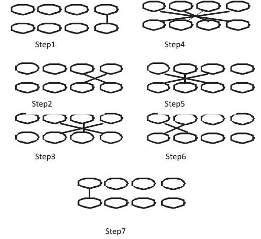
Figure 1. Line Diagram for 4 bit Vedic Multiplication
Parallel Prefix Adder (PPA) is one of the fastest adder (Hoe, Martinez, Vundavalli, 2011) considered among all types of adders. There are different types of PPA's of which, one of them is considered here for implementation of Vedic Multiplier (VM) is Kogge Stone Adder (KSA). It generates the carry signals in O(log n) time(Kumar & Naik, 2014) . It uses group generate and propagate functions. It uses three stages.
i) Pre-processing
ii) Carry look-ahead network
iii) Post-processing
In Pre-processing stage, propagate (p) and generate (g) functions are calculated as,


In Carry look-ahead network, group propagate (cp) and generate (cg) functions are calculated as:-


In Post-processing network, sum and cout is calculated

The schematic for a 16 bit Kogge Stone Adder (KSA) is as shown in Figure 2, (parul and Rahul, 2015) where the black cell represents group propagate and generate function calculation (Harris, 2003) while the grey cell represents the group generate function and the triangle represents buffer where the bit propagates and generate, here the number of carry propagation stages are 4 as given by the equation (6) below:-

where 'n' is the number of carry propagation stages in KSA.
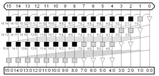
Figure 2. 16-bit Kogge Stone Adder Network
Booth's algorithm is to multiply two binary numbers in signed representation (Booth, 1951) . The algorithm was invented at Birkbeck College, London by Andrew Donald Booth in 1950. The Booth multiplier (BM) reduces the number of partial products by scanning three bits at a time. The first two bits are from the present pair, whereas the last bit is from the adjacent lower order pair. The triplets of bits are examined and are converted by Booth logic into a set of five control signals that is used by the adder cells in the array to control the operations (Goyal, Gupta, Singla, 2014) . The Booth multiplication is used to multiply two signed binary numbers in addition to unsigned numbers. This multiplication of Booth algorithm is as shown in Table 1 to multiply 3 (multiplier, Q) and 7 (multiplicand, M). There are four cycles involved in this case, as the number of bits required to represent 3 and 7 are four, taking the MSB bit as sign bit, i.e. zero. The product obtained is 21 (00010101) stored in A and Q at the last stage.
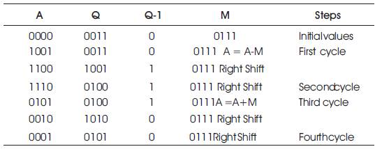
Table 1. Booth Multiplication Algorithm
Firstly, the 2 bit VM has been designed using two half adders & four and gates. The design of 4 bit VM is shown in Figure 3 consists of four 2 bit VM ( R. Anjana et al., 2014) which takes the combination of two 4 bit inputs 'a' and 'b'. The output 'q0-q3' from each 2 bit VM blocks are of 4 bits which are given to KSA of 6 and 4 bit and the combined output of them has been given to KSA of 6 bit to obtain the final output i.e. mul of 8 bit.
Figure 4 shows the design adopted for the implementation (Pohokar et al., 2015) of 8 bit Vedic Multiplier (VM) where the design of 8 bit VM(Mano, 1979) consists of four 4 bit VM which takes the combination of two 8 bit inputs 'a' and 'b'. The output 'q0-q3' from each 4 bit VM blocks are of 8 bits which are given to Kogge Stone Adder of 12 and 8 bit and the combined output of them has been given to Kogge Stone Adder of 12 bit to obtain the final output, i.e., mul of 16 bit.
The design of 16 bit VM consists of four 8 bit VM ( R. Anjana et al., 2014)which takes the combination of two 16 bit inputs 'a' and 'b'. The output 'q0-q3' from each 8 bit VM blocks are of 16 bits which are given to KSA of 24 and 16 bit parallely and the combined output of them has been given to KSA of 24 bit to obtain the final output, i.e. mul of 32 bit as shown in Figure 5.
The Booth implementation(Wakerly, 1999) as shown in Figure 6 consists of different registers A which is initially all zeros, Q as multiplier and Q-1 as a single zero (initial booth bit). The multiplicand (M) and multiplier (Q) are represented by minimum number of binary bits. The MSB bit represents the sign bit i.e., '1' if the number is negative and '0' if positive excluding the minimum requirement of the bits required to represent the number. The last two bits in the representation i.e. A, Q, Q-1 which are Q[0] and Q-1 are examined. Depending upon whether this bits are “00”, “01”, “10”, “11”, the operations mentioned in Figure 6 takes place. The number of checks or steps is equal to the number of bits required to represent the multiplicand and multiplier.
The design of 4 bit Booth Multiplier (BM) consists of the two four bit inputs i.e. multiplicand and multiplier loaded into register M and Q respectively (Goyal, Gupta, Singla, 2014) as per the flowchart in Figure 6. The sequence of steps mentioned in the flowchart takes place and the number of iterations is four for 4 bit BM i.e. the count takes the value from 0000 to 0011.
The design of 8 bit Booth Multiplier (BM) consists of the two eight bit inputs i.e. multiplicand and multiplier loaded into register M and Q as per the flowchart in Figure 6. The sequence of steps mentioned in the flowchart takes place and the number of iterations is eight for 8 bit BM, i.e. the count takes the value from 0000 to 0111.
The design of 16 bit Booth Multiplier (BM) consists of the two sixteen bit inputs i.e. multiplicand and multiplier loaded into register M and Q as per the flowchart. The sequence of steps mentioned in the flowchart takes place and the number of iterations is sixteen for 16 bit BM, i.e. the count takes the value from 0000 to 1111.
The sequence of steps mentioned in the flowchart takes place and the number of iterations is sixteen for 16 bit BM i.e. the count takes the value from 0000 to 1111.
The synthesis of VM (Palnitkar, 1996) has been performed using Xilinx 14.4 ISE & simulation has been done using Isim simulation tool on Spartan 6 family, device Xc6slx45, package as csg324 with speed grade -3. For this configuration, the technology schematic of 16 bit VM using the above implementation method has been shown in Figure 7 with the simulation view of 16 bit VM i.e. the multiplication of two 16 bit unsigned number shown in Figure 8.
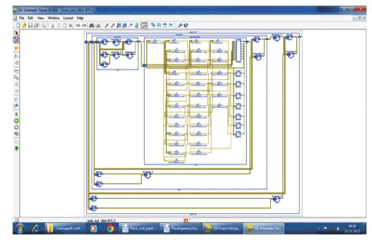
Figure 7. Technology Schematic of 16 bit VM

Figure 8. Simulation Result of 16 bit VM
The technology schematic of 16 bit Booth Multiplier using the above implementation method has been shown in Figure 9 with the simulation view of 16 bit Booth Multiplier i.e. the multiplication of two 16 bit signed as well as unsigned numbers shown in Figure 10.
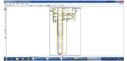
Figure 9. Technology Schematic of 16 bit BM
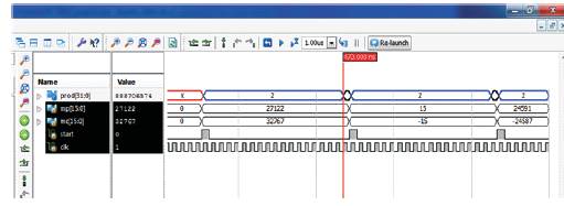
Figure 10. Simulation Result of 16 bit Booth Multiplier
Table 2 shows the synthesis results obtained for VM and Booth Multiplier with the FPGA device Xc6slx45~3csg324 and Figure 11 shows that the synthesis delay comparison graph between Vedic and Booth Multiplier (4/8/16 bit).
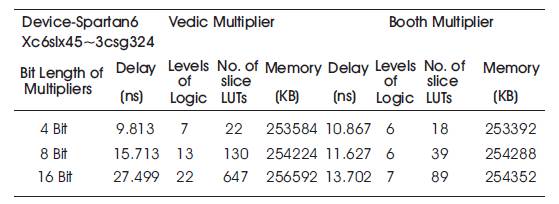
Table 2. Obtained Synthesis Results
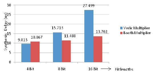
Figure 11. Synthesis Delay Comparison Graph between Vedic and Booth Multiplier (4/8/16 bit)
Based on the hardware, it has been found that the synthesis delay in Booth Multiplier is less compared to VM as the levels of logic or the number of slice LUTs are less in Booth compared to Vedic.
The design of VM based on FPGA implementation using Kogge Stone Adder has been compared with the design of Booth Multiplier implemented. The VMs of 4/8/16 bit has been designed using Kogge Stone Adders of 4/6/8/12/16/24 bit. The Booth Multiplier has also been implemented using the logic in Figure 6. The multipliers have been implemented in Xilinx ISE 14.4. The FPGA implementation has been done in Spartan 6 with the device name as Xc6slx45, package csg324,and speed grade of -3.
It has been found that the delay in Vedic Multiplier (VM) according to synthesis report, is more comparable to Booth Multiplier (BM) as obtained in Table 2. The delay is 9.813 ns for 4 bit VM whereas it is 10.867 ns for BM (4 bit). It can be concluded that for lesser number of bits i.e. 4 bit VM and BM the delay is more in BM, however as the number of bits of multipliers increases as for 8/16 bit VM and BM, the delay is more in VM compared to BM. The delay found in 8 bit VM is 15.713 ns whereas for 8 bit BM it is 11.267 ns. Also for 16 bit VM, the delay is more in VM (27.499 ns) compared to 16 bit BM (13.702 ns) as obtained in the synthesis report of Table 2. The levels of logic obtained in BM is very less compared to VM and thus the synthesis delay based on the hardware. The simulation in BM takes a large waiting time i.e. the output does not respond instantaneously to the change in inputs. There is a minimum wait period of 120 ns, 200 ns, 360 ns for 4, 8,16 bit BM. The BM is a sequential circuit, where the output is obtained when the count value, reaches its maximum value till then the output is in high impedance state or in the waiting period. This is not the case with VM as it is a combinational circuit the output changes immediately with respect to the change in input, there is no waiting period required as in BM. It can thus be concluded that the BM is slower compared to VM.
The VM of different bit lengths (4/8/16 bit) has been designed using Kogge Stone Adders of varying bit lengths requiring higher bits (4/6/8/12/16/24 bit). The BM has been implemented using the flowchart illustrated in Figure 6 and thus it requires the bits of adders that are equal to bit implementation of BM. The number of passes required to implement BM is equal to the number of bits required to represent the multiplicand and multiplier. The MSB bit represents the sign of the number. For example -5 is represented as 011, i.e. minimum three bits and one MSB bit represents its sign as 1011 (-5) in 2's complement notation. The synthesis delay in BM is therefore much less compared to VM (parallel implementation of KSA of higher bit lengths). BM is used to multiply two unsigned as well as signed binary numbers whereas the VM multiplied only unsigned binary numbers, The negative number is stored in 2's complement notation in multiplier (Q) numbers with MSB as sign bit ('1') to represent negative number and positive in multiplicand (M) to multiply two signed binary numbers in Booth algorithm, when both numbers are negative Q and M stores the 2's complement of the numbers with MSB as sign bit ('1') to represent negative number. However the simulation time required in getting the output is much more in BM due to the clock period, whereas the VM responds immediately to the change in input. Therefore, the design used for multiplication should be based on Vedic sutras like Urdhva Trigbhyam (one of the most efficient sutra) which is used here and the fastest PPA, i.e. Kogge Stone Adder.