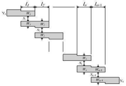
Figure 1. General Structure of Parallel Coupled Micro-strip Band Pass Filter
This paper presents the design of narrow band-pass filter and wide band-pass filter using microstrip coupled line structure. The narrow band-pass filter is designed to operate at dual center frequencies of 1.227 GHz and 1.575 GHz for GPS and the wide band-pass filter to operate at X-band segment (8-12 GHz) of microwave frequency spectrum with center frequency of 10 GHz. The device dimensions are calculated using MATLAB coding and the simulative analysis of the filter is done using ADS and microwave studio software. The filter response by CST and ADS are compared using MATLAB.
The development of wireless technology pacifies the need for RF/Microwave filter with low insertion loss and higher selectivity. The advancement in telecommunication technology gives emphasize on the need of higher frequency band to meet the market needs. A wide frequency band corresponds to large bandwidth and information carrying capacity which can be realized at higher frequencies. At higher frequencies, more antenna gain is possible for a given physical antenna size, which promotes the implementation of miniaturized microwave system. The navigation system and X-band applications both makes use of satellite communication and are used for military purposes. GPS receiver uses band pass filter to select signals within specified bandwidth, reduce harmonics, and improve rejection of interferences for receiver.
Micro-strip line is a good candidate for filter design due its various advantages of low cost, compact size, lightweight, planar structure, and easy integration with other components on a single board.
The objective of this paper is to present the accuracy of the results simulated by 3D simulation software CST Microwave studio with that of numerically simulated software ADS of designed the planar microstrip coupled line filter. The employed design gives more design flexibility over the other designs which involved loading open ends into tunable elements and series tunable sections. The design was simple and easy to implement in the software.
The general structure of parallel coupled microstrip filter illustrate the general notations used for dimensions of coupled line filter. Figure 1 illustrates the coupled line filter that uses half wavelength line resonators that are placed in such a way that the adjacent resonators are parallel to each other along half of their wavelength [ 5].
Figure 1. General Structure of Parallel Coupled Micro-strip Band Pass Filter
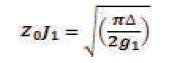
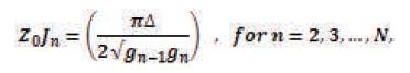
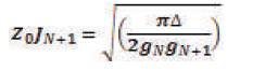
The design equations for a bandpass filter with N+1coupled line sections are given by equations (1), (2), and (3)

In this work, micro-strip narrow bandpass filter of 2nd order coupled line configuration with dual center frequencies of 1.227 GHz and 1.575 GHz, fractional bandwidth of 10% and equal ripple in the pass-band of 0.5 dB using FR4 substrate of dielectric constant of 4.3 and height of 1mm has been designed for GPS application. The element values of Equal-Ripple filter prototypes for 0.5 dB ripple are taken as, g0 =1, g1 =1.4029, g2 =0.7071, g3 =1.9841 for order N=2 [7].
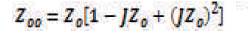
Using equations (3), (4), and (5), some of the design parameters of the three coupled line pairs are calculated and listed in Table 1.
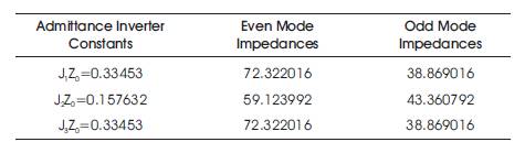
Table 1. Calculated Design Parameters for GPS
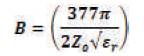
For a single edge Micro-strip line, the even and odd mode impedance is given by equations (6) and (7)


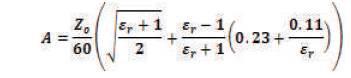
Using single line equations, (w/h)se and (w/h)so from Zose and Zoso has been calculated with εr =4.3. For z0 =50 ohm using equations (9) and (10), A=1.5157033 and B=5.71158 has been evaluated.
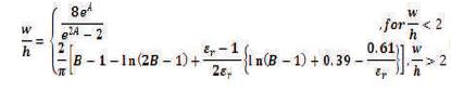
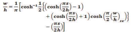
Therefore from equation (8), the value of w/h = 1.94490 has come out for w/h≤2. Therefore w/h≤2 has been chosen.
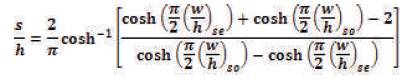
After calculating (w/h)se and (w/h)so , s/h and w/h of each se so desired coupled micro-strip line using equations (11) and (12) has been calculated,
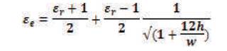
The effective dielectric constant for each coupled line pair has been calculated using equation (13),
The guided wavelength of quasi-TEM mode of edge micro-strip line is determined for each coupled line pair from equation (14) for fc=1.401 GHz
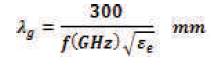
where εe is the effective dielectric constant of micro-stripline.
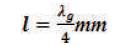
The length of each coupled line section is calculated by,
In this work, micros-strip wide band pass filter of 3rd order coupled line configuration with frequency range of 8-12 GHz, fractional bandwidth of 40% and equal ripple in the pass-band of 0.5 dB using FR4 substrate of dielectric constant of 4.3, and height of 1mm has been designed for X-band application. The element values of Equal- Ripple filter prototypes for 0.5 dB ripple are taken as g0 =1, g1 =1.5963, g2 =1.0967, g3 =1.5963, g4 =1 for order N=3.[1]
Using equations (3), (4), and (5), some of the design parameters of the three coupled line pairs are calculated and listed in Table 2.
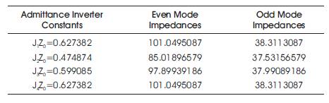
Table 2. Calculated Design Parameters for X band
Using the same procedure, the device dimensions for all the four coupled line pairs has been calculated for fc =10 GHz.
Figure 2 shows the layout of the 2nd order filter designed for GPS having 3 coupled line sections. Figure 3 shows the plot of S21 obtained by simulating the layout by CST software with insertion loss better than 0.02 dB for L1 and L2. The results are then verified by ADS which is a numerically simulated software. Figure 4 shows the plot of S11 having return loss of -12 dB at L1 and -11.5 dB for L2. The results are found to be slightly deviated when compared with ADS.
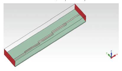
Figure 2. 3D Layout of Edge-coupled Micro-strip Line Filter on CST
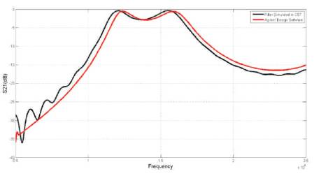
Figure 3. S21 Plot Comparison between CST and ADS for GPS
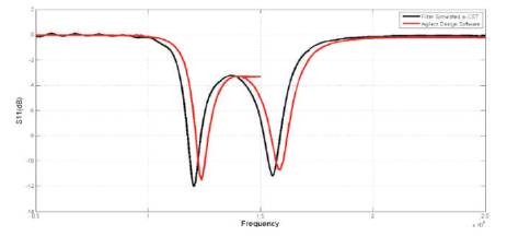
Figure 4. S11 Plot Comparison between CST and ADS for GPS
Figure 5 shows the 3D layout of 3rd order filter designed for X-Band having 4 coupled line sections. Figure 6 shows the plot of S21 in which three resonance peaks are obtained at 8 GHz, center frequency of 10 GHz and 12 GHz with insertion loss better than 0.3 dB. Figure 7 shows the plot of S11 having three resonances with return loss of -27 dB at 8 GHz, -30 dB at 10 GHz, and -34 dB at 12 GHz. The results were then verified with ADS and found to be slightly deviated.
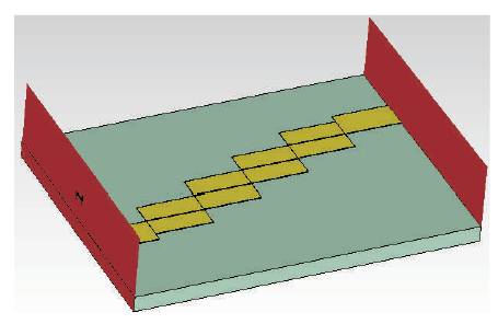
Figure 5. 3D Layout of Edge-coupled Micro-strip Line Filter on CST
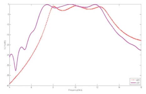
Figure 6. S21 Plot Comparison between CST and ADS
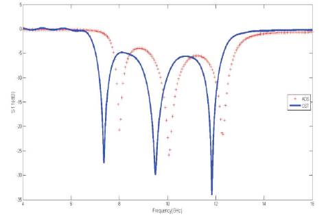
Figure 7. S11 Plot Comparison between CST and ADS for X-band
The device dimensions are mentioned in Table 3 and Table 4 for GPS and X-Band, respectively.
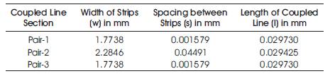
Table 3. Calculated Dimensions of Coupled Micro-strip Line for GPS
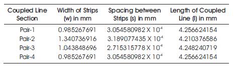
Table 4. Calculated Dimensions of Coupled Micro-strip Line
In this work, the promising results are obtained from narrow dual-band application, followed by an ultra-wideband XBand application band pass filter design using the same technique. The results were satisfactory using ADS software. However, the CST results were showing some amount of deviations with respect to ADS, which is to be studied and needs some improvement in this case.
In the future scope of work, Multi-band applications (Three or more) can be tried using this technique due to simple nature of the technique. Practical implementation of the software design is also to be done so as to establish a confident design. Improvement and miniaturization of the design at low end RF applications is also to be researched using this technique.