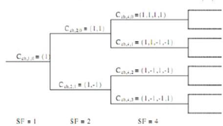
Figure 1. Code tree of Orthogonal Variable Spreading Factor (OVSF) code
This paper describes the wideband Direct Sequence Code Division Multiple Access (WCDMA) wireless transmitter design using Field Programmable Gate Array (FPGA), which has been adopted in many wireless access technologies. Four separate blocks have been designed using digital approach to form the transmitter circuit diagram using the oscillator, the OVSF-code generator, the Parity Check, and the BPSK modulator. The WCDMA air interface was initially designed to support a wide variety of services with different QoS requirements having a maximum bit rate of 2 Mb/s. In order to satisfy the future service and application needs several technical enhancements are being studied and standardized for WCDMA in 3GPP. Wideband Code Division Multiple Access (WCDMA) uses Orthogonal Variable Spreading Factor (OVSF) codes to support diversified data transmission rates and Quality of Service (QoS). In this paper, we propose a improved OVSF code assignment to support QoS for WCDMA.The Synopsys software has been used for the design synthesis and simulation; the Very High Speed Integrated Circuit Hardware Description Language (VHDL) program was used for coding and FPGA for compiling and downloading the simulation. The WCDMA wireless transmitter was designed to transmit with data rates up to 2 Mbps. The transmitted signals were carried with a 40 MHz carrier frequency.
In recent years, there has been a significant amount of research performed in both industry and academia into the development of WCDMA systems. A clear description of a WCDMA has been elusive, since it has a different meaning to every researcher involved in the topic[6]. WCDMA is a type of spread-spectrum communication system in which multiple signal channels occupy the same frequency band, being distinguished by the use of different spreading codes[3]. WCDMA communication is employed in, for example, digital cellular telephone systems and personal communication services. In these systems, a base station communicates with a plurality of mobile stations, one frequency band being used for all of the up-links from the mobile stations to the base station, and another frequency band being used for all of the down-links from the base station to the mobile stations [9]. This paper describes the design and a circuit for pseudo random OVSF coding and synchronization of a wireless transmitter for WCDMA using VHDL software. The circuit for the transmitter is comprised of basic digital components, such as flip-flops, oscillators, shift registers, OVSF coder and a BPSK modulator. FPGA was selected to implement this circuit. The research involved two phases - simulation and synthesis of the VHDL codes using the Synopsys package and converting the integrated circuit of the transmitter in the FPGA compiler for downloading on the Xilinx FPGA board. A VHDL design begins with an ENTITY block that describes the interface for the design. The interface defines the input and output logic signals of the circuit. The ARCHITECTURE block describes the internal operation of the design. Within these blocks, there are numerous other functional blocks used to build the design elements of the logic circuit created. The source code written using the normal TEXT editor, then saved as a VHDL file with '.vhd' extension and transferred to any of the VHDL Design Compilers (DC). If the compilation shows no error(s), the file can be simulated, synthesized and implemented with FPGA. The transmitter components were designed individually using the bottom-up approach. The designs were then combined and defined by a component declaration and port mapping. Generally, this is an easy method although it could have had complications. The basic transmitter circuit used was adopted from the following digital components; flip-flops, shift registers, PN coder and a BPSK modulator with 40 MHz DIP oscillator providing the reference frequency. This paper concentrates on the application of VHDL simulation tool and FPGA compiler to wireless data components. Networks operating over unlicensed bands have recently received increased attention with the prominence of such standards as IEEE 802.11 and Bluetooth. In 3G, the information transferred is not limited to having voices, images and digital data separately. Users will have full coverage and mobility for 144 kbps (preferably 348 kbps) and eventually up to 2 Mbps. With this wide bandwidth, users are able to access the information in full multimedia form, wirelessly and with better quality. The next section of this paper describes the PN code generator, which is the important part of the design. Section 2 presents the transmitter block diagram with the flow chart of the program. Section3 presents language options in creating the design and also the simulation and synthesize tool. Section five presents the hardware implementation.
The idea of the OVSF code is to allow the code words in the CDMA code to have variable lengths, and a higher-rate request is assigned with a single shorter codeword. OVSF codes are defined in the 3GPP standard[1] by the code tree shown in Figure,1. A channelization code CCH,SF,N is uniquely described by two numbers: the spreading factor SF in the range and the identification (ID) number[2]. Each level in the code tree defines channelization codes of length SF as shown in Figure. 1. The control channel is spread by code C256,0, which consists of 256 logic zeros. When only one data channel is transmitted, data channel 1 is spread by code C sf, k where SF is the spreading factor SF, k and k = SF / 4. When more than one data channel is transmitted, all of the data channels have a spreading factor equal to 4.
Figure 1. Code tree of Orthogonal Variable Spreading Factor (OVSF) code
The generation of the OVSF channelization codes is defined in the WCDMA system by three matrix expressions [5]. The direct implementation of these matrix operations requires a significant amount of resources which is convenient only for a software realization based on a microcontroller or a digital signal processor. In order to design an efficient hardware generator for this family of codes, specific properties of OVSF codes are used. The chip sequence is specified in the binary set {+1, –1}, while digital CMOS logic operates on the set {0, 1}. The mapping {“+1” → “logic 0”}and {“–1” → “logic 1”}is therefore adopted as a convention. The spreading codes serve as control signals for a complex ±1 multiplier [2]. In the remainder of the paper, circuits issues are discussed with logic levels of 0 and 1. The binary representation of the ID number describes the trajectory of the code generation along the OVSF code tree shown in Figure 1: a logic 0 for the upper branch or a logic 1 for the lower branch. This property is illustrated by the following example
Example 1: Suppose the channelization code C8,5 is required
SF = 810 = 10002
N = 510 = 01012 = n3 n2 n1 n0
The trajectory of code C8, 5 is defined as follows:
Stage 1 – a single root, always 0
Stage 2 – lower branch, controlled by n2
Stage 3 – upper branch, controlled by n1
Stage 4 – lower branch, controlled by n0
The individual code chips are controlled by corresponding bits in the ID number. The OVSF chips can therefore be produced by a XOR operation over certain bits of the code ID number. The participation of a specific bit in the XOR operation is periodic in time and can be controlled by a binary counter as listed in Figure 2. Based on observations of the data listed Figure 2, logic level architecture of an OVSF code generator is shown in Figure 3. The Least Significant Bit (LSB) of the counter enables the MSB of N, bit n2, to be included in the XOR operation. The MSB of the counter controls n0, which is the LSB of N.
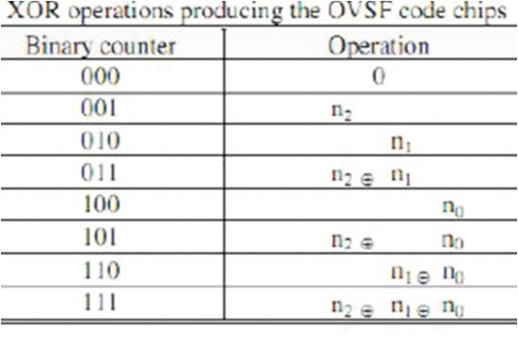
Figure 2. XOR operation producing the OVSF code chips
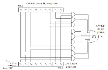
Figure 3. OVSF code generator
The WCDMA standard, however, specifies that the code generator should be capable of producing codes with a variable spreading factor over the range SF = 4 to 512 [7]. The issue is how best to match the number N and the binary counter in reverse order for different spreading factors. Two techniques are suggested to accomplish this objective:
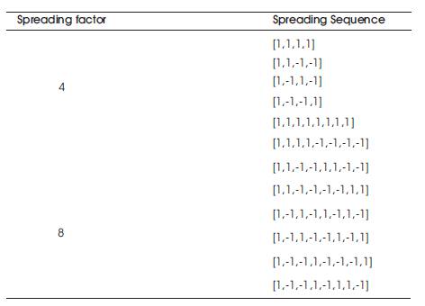
Table. Spreading Factor and their Spreading Sequence
Code blocking leads to an increase in call blocking rate for higher data rate users and a reduction in spectral efficiency[4,10]. It is evident from the code tree in Figure .1 that the higher is the re-quested data rate, the larger is the blocking probability. To circumvent this problem, the author propose a scheme that dynamically reassigns OVSF codes and, as a result, code blocking is completely eliminated. This scheme is optimal in the sense that it minimizes the number of OVSF codes that must be reassigned to support a new call. As the name suggest, the allocated codes are dynamic in nature in the sense that a particular session may start transmitting with a particular OVSF code and end its session with a different code. As earlier stated, if the available assignable codes satisfy the Kraft's inequality it implies that the call can be supported by the channelization code. In the event where there is no single code available to support this particular call session as explained in example 1 above, a reassignment of codes takes place to create room to accommodate this call. The spreading code of one or more calls are interchanged with new codes so that an assignable code that meet the spreading and orthogonality requirements of the new call is created thereby[9]. The DCA [2] ensures efficient use of the channel resources with more throughput and little blocking but comes with it an additional signaling and delay[8,11].
The input interfaces will be responsible for communicating with peripheral components that the user can interact with the serial communication interface will be responsible for transport of data between the two FPGA boards. The transmitter will be responsible of spreading the signal before the data is sent as shown in Figure 4. The receiver will be responsible for frame synchronization and dispreading the signal before data is received as shown in Figure 5. The timing controller—Clock Master as in our design, will coordinate the timing relationship with other parts of the system to initialize, to maintain, and to terminate the communication between users and base station. The frame builder and frame analyzer are responsible for assembling the data frame and disassemble the frame. When one user is turned on, that user is sending a channel access request. A frame is constructed with the Random Access Request code in the Channel Header. Each bit after the sync code is spread and the frame is transmitted from the mobile user board to the base station board. When the base station board receives the frame, it must first find the sync code. Once this is accomplished, the rest of the data frame is de-spreaded. The channel header is analyzed and if it recognizes the Random Access Request, an LED on the base station lights and another frame is constructed with the Acknowledge code in the Channel Header. Each bit after the sync code is spreaded and the frame is transmitted from the base station board to the mobile user board. When the mobile user board receives the frame, it finds the sync code, and de-spreads the rest of the frame. If the Acknowledge signal is recognized in the frame, an LED is lit on the mobile user board, the channel enters communication mode and is ready to receive keypad input and transmission.
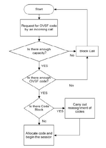
Figure 4. DCA Flow Chart
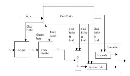
Figure 5. Transmitter Block Diagram
When the user presses a key on his keypad, a frame is created containing the Communication Send code in the Channel Header, and the user data information. Each bit after the sync code spreads over the scrambling code and the data frame is transmitted from the mobile station board to the base station board. When the base station board receives the frame, it finds the sync code, and de-spreads the rest of the frame. The frame is disassembled and analyzed. If the Communication Send code is detected, the data portion of the frame is displayed on the display. Another frame is constructed with the Communication Send code in the Channel Header and the user data is echoed in the data portion of the frame. Each bit after the sync code is spread and the data frame is transmitted from the base station board to the mobile user board. When the mobile user board receives the frame, it finds the sync code, and dispreads the rest of the frame. If the Communication Send signal is recognized in the frame, the LCD for the particular user displays the data.
The user turns off their switch to terminate their connection. The user's is extinguished on the mobile user board, the Display is cleared and the keypad is no longer functional for the specified user. A close frame is generated in the mobile user board when both users are offline, spreads and then transmitted to the base station. The base station despreads the frame, analyzes the frame and releases any system resources and clears any display output
The VHDL source code files were already created and saved in the same folder, all with the extension '.vhd'. A toplevel design was created for the transmitter and receiver for the whole design. Then the WCDMA Transmitter and Receiver design was simulated and synthesized to check its logical operation. The individual elements were simulated using vhdlan and vhdlsim in the DOS command for Windows NT. The FPGA Compiler was used for compiling and synthesizing the VHDL source code. The synthesis allowed the timing factors and the other influences of the actual FPGA devices to affect the simulation, thereby resulting in a more thorough check before the design was committed to the FPGA. The results of this simulation and synthesis are the FPGA optimized chip. Test-bench files were created to test all the above files. The purpose of a test bench is to verify the functionality of a model or package. Figure 7 shows the input and output ports of the transmitter and receiver section. The FPGA optimized chip for the transmitter is shown in Figure 7. The final result waveform from the created test bench for the top-level design is shown in Figure 8. The WCDMA wireless transmitter was designed to transmit data with higher data rates of 2 MHz was selected as the clock rate to come out with 2 Mbps data rate.
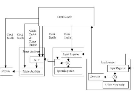
Figure 6. Receiver Block Diagram
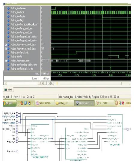
Figure 7. Synthesis Result for WCDMA Transmitter
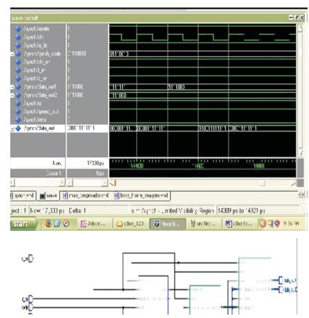
Figure 8. Synthesis Result for WCDMA Receiver
There are several ways to implement a reconfigurable radio terminal but one that offers a wide application flexibility, ranging from high computational intensive tasks to algorithmically complex but relatively low speed tasks, and at the same time flexibility to modify its behaviour, is the one based on FPGAs. Their increasing capacity and speed, together with the progressive reduction of power consumption make of them a good candidate to occupy relevant positions in future radio terminals designed under the Software Radio line of thought. A WCDMA system taking advantage of the structural properties of FPGAs has been designed to check their adaptation to that kind of application and to explore the pros and cons when designing specific parts. Like in many digital systems here appears a trade-off between speed and logic resources used: higher is the speed required, higher are the resources required to implement the functions.