Figure 1. SAR Type ADC
In this paper, in order to meet the needs of Wireless Access in Vehicular Environment applications, Analog-to-Digital converter with 10 bit 40 MS/s (Mega Samples per second) has been introduced. The ADC planned here is to be compelled to be operate at high varying temperatures under the given constraints. To implement the system, the design was changed by reducing the gratuitous building blocks that the area unit provides within the existing design. The non - essential building blocks area unit comprises reference drivers, Sample and Hold Applications (SHA), level shifters, etc. In the planned design there is a tendency to take away these building blocks and introduce the internal signal amplification technique. This amplification technique extends the effective signal by varying each multiplying data converter and flash ADC, in addition to that, the error correction vary. The new clock generation circuit for a SHA-less pipelined ADC removes the requirement of a better frequency external clock. The prototype ADC was fabricated in a 32-nm CMOS process. The design is developed by using the backend tool HSPICE Design suite and Virtex6 FPGA for hardware Prototyping Environment. The Design summary and simulation waveforms show that the proposed Architecture consumes low power and work with high performance.
Automobiles became an important a part of human life nowadays, where several studies were being actively conducted to make cars a lot of convenient and intelligent for safety and traffic management, which is still delineated by the Intelligent Transportation System (ITS). Among the specified varied technologies for ITS, wireless communications is one of the key parts. The IEEE 802.11p for Wireless Access in Vehicular Equipment (WAVE) systems define specifications for vehicle-to-vehicle and vehicleto- infrastructure communications. A WAVE system encompasses a channel information measure of 5 to 20 megacycle and a carrier frequency of around 5.9 GHz ( IEEE Standard for Information Technology, 2010; Jiang and Delgrossi, 2008
The design was requested to possess a resolution of ten bits and a sample rate of 40 MHz. Presently, ADCs with such specifications will be enforced with terribly low power consumption (Cho et al., 2011). However, recent mobile electronic devices like good phones that ought to consume less power are considered to be potential, which is a facility constraint for automobile-applications ( Aijaz et al., 2006; Yousefi et al., 2006) to be principally used for driving. Instead of mandating low-power operation, they need to be reliable even in extreme environments like highly regarded and cold temperatures. A WAVE module ought to work correctly during a temperature varation from -40º C to 125 º C, that corresponds to the grade-1 level of the AEC-Q100 standards (Stress Test Qualification for Integrated Circuits, 2007). Considering this reliablily issue. AN operational amplifier device (op-amp)-based pipelined ADC has been chosen as a result of the feedback-based residue amplification. It has been tested to be reliable through the long history of solid-state circuits, in distinction with different sorts like sequential approximation register for ADCs that does not any residue amplification; so accuracy might suffer from the comparator offset drift (Tewksbury and Lee, 1994)
This paper proposes many circuit techniques to produce reliable operation with a pipelined ADC under the given constraints like totally different supply voltages for analog/digital circuits and a little signaling variation. so as to forestall the nonessential building blocks from lowering the circuit yield, and the ADC is simplified by removing reference drivers and also the frontend Sample and Hold Amplifier (SHA). The projected internal signal amplification technique adjusts the effective signal variation to correspond with the provision level by the misbehaving capacitors alone and therefore extends that the error varies for every flash sub ADC. Additionally, the projected internal sample clock generator eliminates the necessity for a twice-frequency external clock (Cho and Lee, 2005).
The rest of the paper is organized as follows; ADC and ADC types are discussed in section 1 and section 1.1 respectively. Section1.2 focuses on applications of ADC while the Existing architecture is pointed in section 2. The importance of the proposed structure and its functionality is outlined in section 3 of this document followed by Simulation and Synthesis results are evaluated in section 4. Finally the paper is concluded.
An Analog-to-Digital Converter (ADC), is a device that converts a continuous physical quantity (usually voltage) to a digital number that represents the quantity's amplitude. This conversion involves quantization of the input, so it necessarily introduces a small amount of error. Instead of doing a single conversion, an ADC often performs the conversions ("samples" the input) periodically. The result is a sequence of digital values that have been converted from a continuous-time and continuous-amplitude analog signal to a discrete-time and discrete-amplitude digital signal. An ADC is defined by its bandwidth (the range of frequencies it can measure) and its signal to noise ratio (how accurately it can measure a signal relative to the noise it introduces). The bandwidth of an ADC is characterized primarily by its sampling rate, and to a lesser extent by how it handles errors such as aliasing. The dynamic range of an ADC is characterized by many factors, which includes resolution, linearity, and accuracy. This ADC is also characterized by effective number of Bits (ENOB). ENOB has a resolution equal to that of an Ideal ADC. Typically ADCs are taken to match the bandwidth, and the signalto- noise ratio. If the chosen ADC is operates at a sampling rate greater than double the bandwidth of the signal, then a perfect re-modification is possible for a given ADC and this can be capable of not considering Quantization errors.
The presence of quantization error limits the dynamic range of even an ideal ADC, however, if the dynamic range of the ADC exceeds that of the input signal, its effects may be neglected resulting in an essentially perfect digital representation of the input signal. An ADC can also give AN isolated measure like AN device that converts AN input analog voltage or current to a digital range proportional to the magnitude of the voltage or current. However, some non-electronic or solely partly electronic devices, like rotary encoders, may be thoughtabout ADCs. The digital output could use totally different cryptography schemes. Usually the digital output are going to be a two's complement binary range that is proportional to the input, however measure alternative potentialities. An encoder, for instance, would possibly output a grey code.
It has a bank of comparators sampling the input signal in parallel, each resposible for their decoded voltage range.
It uses a comparator to successively narrow a range that contains the input voltage
It produces a saw-tooth signal that ramps up or down then quickly returns to zero.
The Wilkinson ADC is based on the comparison of an input voltage with that produced by a charging capacitor.
It (also dual-slope or multi-slope ADC) applies the unknown input voltage to the input of an integrator and allows the voltage to ramp for a fixed time period (the runup period).
A delta encoded ADC or counter-ramp has an up-down counter that feeds a digital to analog converter (DAC).
It (also called sub- ranging quantizer) uses two or more steps of sub-ranging.
It also known as a delta-sigma ADC over samples the desired signal by a large factor and filters the desired signal band.
It uses M parallel ADCs, where each ADC samples data every Mth cycle of the effective sample clock.
In DSP, ADCs are used to send the Analog data in the form of Digital so data that error rates can be minimized and no losses occur during the transmission. ADCs are also used to process the data, store the information, and used in TV tuner cards for fast video conversions. Moreover, ADCs are commonly used in microcontrollers of bit size, such as 8,10,12,16 bits. ADCs in Digital Signal Processing (DSP) lead to its applications to enhance memory (data) size.
Digital imaging systems usually use Analog-to-Digital Converters in digitizing pixels. Some measuring systems usually use Analog-to-Digital Converters to convert signal strength to digital values for resulting in a signal process. Several alternatives in place and remote sensing systems usually use analogous technology. The amount of binary bits within the ensuing digitized numeric values reflects the resolution, the amount of distinctive separate levels of division (signal processing). There is a correspondence between the analog signals and therefore the digital signal depends on the division error. The division method should occur at an adequate speed, a constraint which will limit the resolution of the digital signal. Several sensors use analog signal, such as temperature, pressure, pH, intensity level, etc., and are fed to an ADC to supply a digital range proportional to the signaling.
Analog-to-Digital Converters are capable of integrating current music reformation methodology. To generate music on computers using an Analog recording system, people therefore need Analog-to-Digital converters to create pulse code modulation that read on the Compact Discs and Digital music files.
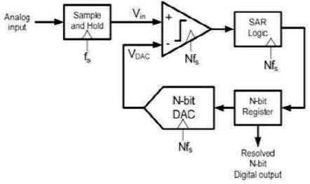
The algorithm used in Successive Approximation is based on a binary search algorithm, and this is more component efficient than Flash ADCs, which use a brute force approach to perform data conversion. Figure 1 illustrates the topology of a standard Successive Approximatic Register (SAR) ADC. In a SAR ADC, the analog input is sampled by a sample-and-hold circuit, which operates at the effective Nyquist sampling rate of the ADC.
Figure 1. SAR Type ADC
The significant advantage of the SAR ADC is that it uses only a few analog components (only a single comparator) to implement N-bit data conversion, resulting in a compact area and simple design. Furthermore, since the topology produces a new digital output every 1/f8 , the latency of the ADC with respect to s the sampling rate is only one clock cycle of the Nyquistrate clock f8.
As a result the SAR topologies are often helpful in systems that need ADCs in feedback. The numerous advantage of the SAR ADC is that it uses solely a number of analog parts (solely one comparator) to implement N-bit conversion, leading to a compact space and easy style.
Pipelined ADCs shown in Figure 2 are capable of resolving medium to high resolutions like the SAR ADC topology, however unlike the SAR topology the pipelined approach is able to achieve very high sampling rates as it does not require a large clock frequency to realize high resolution conversion. During the first clock cycle the N/2 most significant bits are resolved (where N is the number of bits in the final ADC output). During the second clock cycle the resolved N/2 MSBs are removed from the input, the residue amplified by 'A' to full scale to maintain the dynamic range, and reuse reference voltages, and subsequently the remaining N/2 bits are resolved.
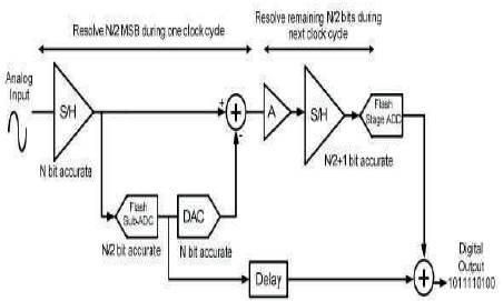
Figure 2. Pipelined ADC
In this work, the ADC is given with supply voltage of 3.3 V and 1.8 V, respectively and the input signal range was given as 0.7 to 1.7 V and the topology is shown in Figure 3. In topology shown in Figure 3, two attached reference drivers were used (Cho and Lee, 1994) for 0.7 and 1.7 V with circuit complexity and power consumption, a single regulated 1.8 V internal supply is generated from the 3.3 V external supply through a simple regulator for both the analog supply and the reference driver (i.e., supply referencing). Thus the simplified deign style reduces circuit quality and reduces the possibility of performance degradation that would have occurred with sophisticated reference drivers below extreme environmental variations in method; provide voltage, and temperature (PVT).
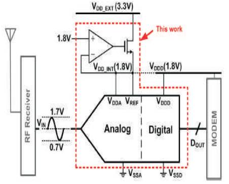
Figure 3. ADC with Regulator based Supply Referencing
In addition, circuit level matching between the Analog and Digital circuits removes the necessity for interfacing level shifter logics between them, and additionally enhances the strength of the circuit operation underneath PVT variation. Level shifting logic will fail to retort to its input once an outsized voltage distinction exists between the Analog and Digital blocks (Koo et al., 2005). The massive fall from 3.3 to 1.8 V, the regulator can be designed with a single-stage telescopic Op-amp and a supply follower output stage that has wide information measure with comparatively low power consumption. But the problem associated with Figure 3 is that full voltage is smaller than the reference voltage, which is 1.8 V (Choi et al., 2006). So there is a necessity for internal Amplification.
Figure 4 shows the modified block diagram of supply referencing 10 bit pipelined ADC with internal signal, which is built with amplified Multiplying Analog-to-Digital Converter (MDAC) (Stroeble et al., 2006) and flash Sub- ADC at the stage one of the circuit. This modification leads to reducing the output swings. Due to the involvement of more capacitors in the structure shown in Figure 4, the major limitation is reduced feedback factor and low performance in loop gain and bandwidth. This problem is again rectified by using capacitive level shifters (Ryu et al., 2007). In all these, the capacitance and Op-amps have common mode feedbacks similar to the structure (Yang et al., 2012). Further the metal finger type capacitors (Harpe et al., 2011) are widely used for perfect matching capability.
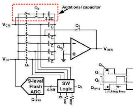
Figure 4. MDAC with Internal Signal Amplification
Most conventional Sample-and-Hold Amplifier SHA-less pipelined ADCs use a clock that is two times faster than the ADC's conversion frequency (Jeon et al., 2007). To remove this extra requirement, the presented design in Figure 5 provides a clock generator that generates the sampling clock on hip from an external clock that has the same frequency as the A/D conversion rate. The sampling time skew between the first stage MDAC and the sub-ADC in a SHA-less pipelined ADC produces a dynamic offset error, particularly when the input frequency is high.
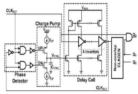
Figure 5. SHA-less Pipelined ADC
To make the use of Pipelined ADC to a larger extent in the field of Digital Signal Processing, Speech, Video recording, and Communications, effective hardware description tools are used. In this paper, the authors use HSpice as a software tool to analyze the working principles of ADC. Since the paper consists of MOS transistors and more number of logic gates, the backend tools like Microwind, Mentor graphics tool, and Tanner tools are preferred, but in this paper H-spice tool provides a simple platform to make the analysis of Pipelined ADC. The simulation waveform illustrated in Figure 6 shows the Analog-to-Digital Converter without pipelining. The delay associated without pipelined ADC is shown in Figure 7, which reveals the fact that existing architecture has a delay of 15 to 16 seconds. The waveforms strengthen the fact that circuit topology is not efficient to generate outcome as the result suffers with glitches (noise or unwanted disturbances).
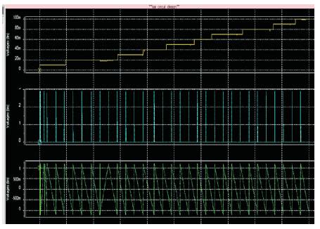
Figure 6. ADC without Pipeline (Simulation)
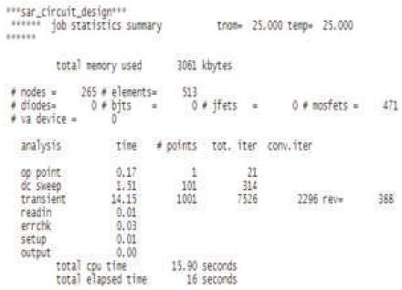
Figure 7. ADC Without Pipeline(Delay Factor)
As mentioned in the proposed structure that the limitations in the existing architecture is rectified and this can be proved with the following waveforms shown in Figure 8. On observing the obtained waveforms, it clearly reflects the mark that the glitches are overcome with the SHA-less Pipelined ADC and produces better results than the existing methodology. Figure 9 strengthens the comments of proposed architecture as it clearly shows the delay time to execute the output is 11 seconds than that of 16 seconds.
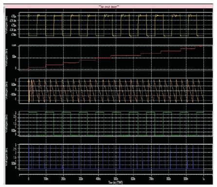
Figure 8. SHA-less Pipelined ADC (Simulation)
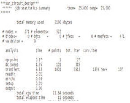
Figure 9. SHA-less Pipelined ADC(Delay Factor)
H-spice is a backend tool used in this work to analyze the process. The experimental results shown in Table 1 proves the effectiveness of the proposed technique with good performance for WAVE applications.
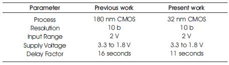
Table 1. Comparison of Results
In this paper, a 10-bit pipelined ADC for IEEE 802.11p for WAVE applications has been described. The design is modeled with referencing simplified circuits with no reference drivers, SHA, or level shifters, and by virtue of the use of internal signal amplification technique, moreover this developed prototype ADC Architecture even operates at high temperatures. This work eliminates the need of two clock generators, thereby reduces the transistor count. VLSI mainly focuses on Area, Delay, and Power consumption, and there is a tradeoff between these parameters. This work focuses on efficient communication between vehicular environments.