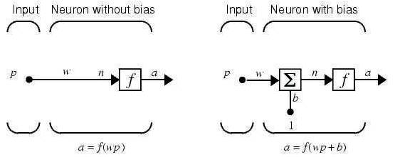
Figure 1. Neuron with single input
In this paper, an optimized high speed parallel processing architecture with pipelining for multilayer neural network for image compression and decompression is implemented on FPGA (Field-Programmable Gate Array). The multilayered feed forward neural network architecture is trained using 20 sets of image data based to obtain the appropriate weights and biases that are used to construct the proposed architecture. Verilog code developed is simulated using ModelSim for verification. The FPGA implementation is carried out using Xilinx ISE 10.1. The implementation is performed on Virtex-5 FPGA board. Once interfacing is done, the corresponding programming file for the top module is generated. The target device is then configured, programming file is generated and can be successfully dumped on Virtex-5. The design is then analyzed using Chip Scope Pro. The Chip Scope output is observed. The output is successfully compared with VCS (Verliog Compiler Simulator) simulation output. The design is optimized for power of 1.01485 W and memory of 540916 KB.
Artificial Neural Networks (ANN) [1] for image compression applications has marginally increased in recent years. Neural networks are inherent adaptive systems; they are suitable for handling nonstationaries in image data. Artificial Neural Networks can be employed with success to image compression. Image Compression Using Neural Networks by Ivan Vilovic[2] reveals a direct solution method for image compression using the neural networks. An experience of using multilayer perceptron for image compression is also presented. The multilayer perceptron is used to transform coding of the image. Image compression with neural networks by J. Jiang[3] presents an extensive survey on the development of neural networks for image compression, which covers three categories: direct image compression by neural networks, neural network implementation of existing techniques, and neural network based technology which provide improvement over traditional algorithms.
Neural Networks-based Image Compression System by H. Nait Charif and Fathi. M. Salam[4] describes a practical and effective image compression system based on multilayer neural networks. The system consists of two multilayer neural networks that compress the image in two stages. The algorithms and architectures reported in these papers sub divided the images into sub blocks and the sub blocks are reorganized for processing. Reordering of sub blocks leads to blocking artifacts. Hence it is required to avoid reorganization of sub blocks. Although there is no significant work on neural networks that can take over the existing technology, there are some admissible attempts. Research activities on neural networks for image compression do exist in many types of networks such as - Multi-Layer Perceptron (MLP) [5-16], Hopfield[17], Self-Organizing Map (SOM), Learning Vector Quantization (LVQ) [18,19], and Principal Component Analysis (PCA) [20]. Among these methods, the MLP network, which usually uses back propagation training algorithm provides simple and effective structures. It has been more considered in comparison with other artificial neural network (ANN) structures. The compression of images by Back-Propagation Neural Networks (BPNN) is investigated by many researchers. One of the first trials in using this approach was done in[6], in which the authors proposed a three layer BPNN for compressing images. In their method, original image is divided into blocks and fed to input neurons, compressed blocks are found at the output of the hidden layer and the de-compressed blocks are restored in the neurons of the output layer.
Neural networks are composed of simple elements operating in parallel. These elements are inspired by biological nervous systems. As in nature, the connections between elements largely determine the network function. The Neural network can be trained to perform a particular function by adjusting the values of the connections (weights) between elements. Typically, neural networks are adjusted, or trained, so that a particular input leads to a specific target output.
Neural networks have been trained to perform complex functions in various fields, including pattern recognition, identification, classification, speech, vision, and control systems. Neural networks can also be trained to solve problems that are difficult for conventional computers or human beings. Neural networks, with their remarkable ability to derive meaning from complicated or imprecise data, can be used to extract patterns and detect trends that are too complex to be noticed by either humans or other computer techniques[16]. A trained neural network can be thought of as an "expert" in the category of information it has been given to analyze. A neuron with a single scalar input [2] and no bias appears on the left as shown in Figure 1.
The scalar input p is transmitted through a connection that multiplies its strength by the scalar weight w to form the product wp, again a scalar. Here the weighted input wp is the only argument of the transfer function f, which produces the scalar output a. The neuron on the right has a scalar bias, b. It can be viewed that the bias is simply being added to the product wp as shown by the summing junction or as shifting the function f to the left by an amount b. The bias is much like a weight, except that it has a constant input of 1.
The transfer function in net input n, again a scalar, is the sum of the weighted input wp and the bias b. This sum is the argument of the transfer function f. Here f is a transfer function, typically a step function or a sigmoid function, that takes the argument n and produces the output a. The parameters w and b are both adjustable scalar parameters of the neuron. The central idea of neural networks is that such parameters can be adjusted so that the network exhibits some desired or interesting behavior. Thus, the network can be trained to do a particular job by adjusting the weight or bias parameters, or perhaps the network itself will adjust these parameters to achieve some desired end.
Figure 1. Neuron with single input
Three of the most commonly used functions are as follows: The hard-limit transfer function shown in Figure 2 limits the output of the neuron to either 0, if the net input argument n is less than 0, or 1, if n is greater than or equal to 0. Figure 3 illustrates the linear transfer function.
Neurons of this type are used as linear approximations in Linear Filters.
The sigmoid transfer function shown in Figure 4 takes the input, which can have any value between plus and minus infinity, and squashes the output into the range 0 to 1.
This transfer function is commonly used in back propagation networks, in part, because it is differentiable. The symbol in the square to the right of each transfer function graph represents the associated transfer function. These icons replace the general f in the boxes of network diagrams to show the particular transfer function being used.
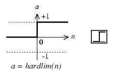
Figure 2. Hard-limit Transfer Function
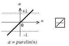
Figure 3. Linear Transfer Function
A neuron with a single R-element input vector is shown in Figure 5. Here, the individual element inputs P1, P2, P3,…..PR are multiplied by weightsW1,1, W1,2,……W1,R and the weighted values are fed to the summing junction. Their sum is simply Wp, the dot product of the (single row) matrix W and the vector p.
The neuron has a bias b, which is summed with the weighted inputs to form the net input n. This sum, n, is the argument of the transfer function f as shown in equation (1.1).
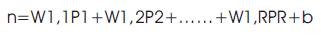
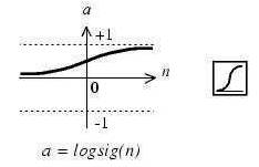
Figure 4. Log- sigmoid Transfer Function
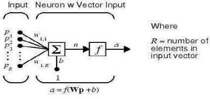
Figure 5. Neuron with a single R-element input vector
When networks with many neurons are considered, and perhaps layers of many neurons, the abbreviated notation for an individual neuron is as shown in Figure 6.
Here the input vector p is represented by the solid dark vertical bar at the left. The dimensions of p are shown below the symbol p in the figure as Rx1. Thus, p is a vector of R input elements. These inputs postmultiply the singlerow, R-column matrix W. As before, a constant 1 enters the neuron as an input and is multiplied by a scalar bias b. The net input to the transfer function f is n, the sum of the bias b and the product Wp. This sum is passed to the transfer function f to get the neuron's output a, which in this case is a scalar. If there were more than one neuron, the network output would be a vector.
A layer includes the combination of the weights, the multiplication and summing operation (here realized as a vector product Wp), the bias b, and the transfer function f. The array of inputs, vector p, is not included in or called a layer. Each time this abbreviated network notation is used, the sizes of the matrices are shown just below their matrix variable names. This notation allows to understand the architectures and follow the matrix mathematics associated with them.
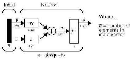
Figure 6. Abbreviated notation for an individual neuron
Two or more of the neurons can be combined with a layer, and a particular network could contain one or more such layers. A single layer of neurons is considered.
A one-layer network with R input elements and S neurons is as shown in Figure 7. In this network, each element of the input vector p is connected to each neuron input through the weight matrix W. The ith neuron has a summer that gathers its weighted inputs and bias to form its own scalar output n(i). The various n(i) taken together form an Selement net input vector n. Finally, the neuron layer outputs form a column vector a. The expression for a is shown at the bottom of Figure 7.
It is common for the number of inputs to a layer to be different from the number of neurons (i.e., R is not necessarily equal to S). A layer is not constrained to have the number of its inputs equal to the number of its neurons. A single (composite) layer of neurons can be created by having different transfer functions, simply by putting two of the networks in parallel. Both networks would have the same inputs, and each network would create some of the outputs.
The input vector elements enter the network through the weight matrix W.
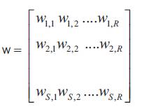
The row indices on the elements of matrix W indicate the destination neuron of the weight, and the column indices indicate which source is the input for that weight. Thus, the indices in w1,2 say that the strength of the signal from the second input element to the first (and only) neuron is w1,2. The S neuron R input one-layer network also can be drawn in abbreviated notation as shown in Figure 8.
Here p is an R length input vector, W is an SxR matrix, and a and b are S length vectors. As defined previously, the neuron layer includes the weight matrix, the multiplication operations, the bias vector b, the summer, and the transfer function boxes.
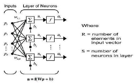
Figure 7. One-layer network with R input elements and S neurons
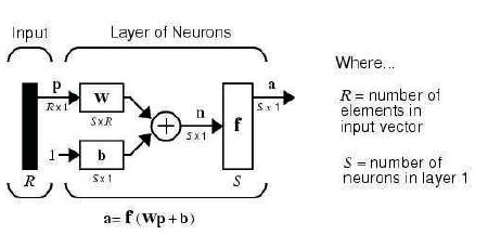
Figure 8. Abbreviated notation for S neuron R input one-layer network
A network can have several layers. Each layer has a weight matrix W, a bias vector b, and an output vector a. To distinguish between the weight matrices, output vectors, etc., the number of the layer is appended as a superscript to the variable of interest. This layer notation can be used in the three-layer network as shown in Figure 9.
The network shown below has R1 inputs, S1 neurons in the first layer, S2 neurons in the second layer, etc. It is common for different layers to have different numbers of neurons. A constant input 1 is fed to the bias for each neuron. The outputs of each intermediate layer are the inputs to the following layer. Thus layer 2 can be analyzed as a onelayer network with S1 inputs, S2 neurons, and an S2xS1 weight matrix W2. The input to layer 2 is a1; the output is a2. Now that all the vectors and matrices of layer 2 have been identified, it can be treated as a single-layer network on its own. This approach can be taken with any layer of the network.
The layers of a multilayer network play different roles. A layer that produces the network output is called an output layer. All other layers are called hidden layers. The threelayer network shown has one output layer (layer 3) and two hidden layers (layer 1 and layer 2). It is also referred to as a fourth layer. The same three-layer network can also be drawn as shown in Figure 10 using abbreviated notation.
Multiple-layer networks are quite powerful. For instance, a network of two layers, where the first layer is sigmoid and the second layer is linear, can be trained to approximate any function arbitrarily well.
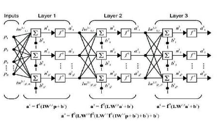
Figure 9. Three-layer network
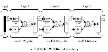
Figure 10. Abbreviated notation for Three-layer network
Network inputs might have associated processing functions. Processing functions transform user input data to a form that is easier or more efficient for a network. For instance, mapminmax transforms the input data so that all values fall into the interval (-1, 1). This can speed up learning for many networks. Removeconstantrows removes the values for input elements that always have the same value because these input elements are not providing any useful information to the network. The third common processing function is fixunknowns, which recodes unknown data (represented in the user's data with NaN values) into a numerical form for the network. Fixunknowns preserves information about which values are known and which are unknown.
Similarly, network outputs can also have associated processing functions. Output processing functions are used to transform user-provided target vectors for network use. Then, network outputs are reversed-processed using the same functions to produce output data with the same characteristics as the original user-provided targets. Both mapminmax and removeconstantrows are often associated with network outputs. However, fixunknowns is not associated. Unknown values in targets (represented by NaN values) do not need to be altered for network use.
A single-layer network of S logsig neurons having R inputs is shown in Figure 11 in full detail on the left and with a layer diagram on the right. Feedforward networks often have one or more hidden layers of sigmoid neurons followed by an output layer of linear neurons. Multiple layers of neurons with nonlinear transfer functions allow the network to learn nonlinear and linear relationships between input and output vectors. The linear output layer lets the network produce values outside the range -1 to +1.
On the other hand, if the outputs of a network need to be constrained (such as between 0 and 1), then the output layer should use a sigmoid transfer function. For multiplelayer networks, the number of layers determines the superscript on the weight matrices. The appropriate notation is used in the two-layer network shown in Figure 12.
This network can be used as a general function approximator. It can approximate any function with a finite number of discontinuities arbitrarily well, given sufficient neurons in the hidden layer.
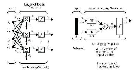
Figure 11. Single-layer network of S logsig neurons having R inputs
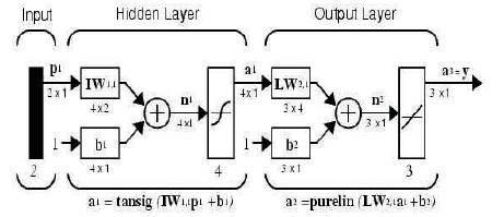
Figure 12. Two-layer tansig/purelin network
The first step in training a feedforward network is to create the network object. The function newff creates a feedforward network. It requires three arguments and returns the network object. The first argument is a matrix of sample R-element input vectors. The second argument is a matrix of sample S-element target vectors. The sample inputs and outputs are used to set up network input and output dimensions and parameters. The third argument is an array containing the sizes of each hidden layer.
More optional arguments can be provided. For instance, the fourth argument is a cell array containing the names of the transfer functions to be used in each layer. The fifth argument contains the name of the training function to be used. If only three arguments are supplied, the default transfer function for hidden layers is tansig and the default for the output layer is purelin. The default training function is trainlm.
The function newcf creates cascade-forward networks. These are similar to feed-forward networks, but include a weight connection from the input to each layer, and from each layer to the successive layers. The three-layer network also has connections from the input to all three layers. The additional connections might improve the speed at which the network learns the desired relationship.
The simout values are obtained for every signal given as input to the FIR (First impulse Response) filter. Simout values obtained, for every signal, from matlab workspace are then given as input to Neural Network Algorithm, developed in matlab, for training. Neural Network is tested with filter. Generated waveform for given input values is as shown in Figure 13. It shows all the four input signals given as input to the Neural Network Algorithm. The algorithm performs the required training on the input signals. The Neural Network Training (nn train tool) is as shown in Figure 14.
The neural network output after training is as shown in Figure 15.
The generated Feed Forward Neural Network is as shown in Figure 16. The co-efficients of this network are obtained from the matlab command window. The co-efficients obtained are Input Weights (IW), Layer weights (LW) and biases b(1) & b(2). A verilog code is developed for the network and is implemented on FPGA. The Input weights (IW), Layer weights (LW) and biases b(1) & b(2) are given as inputs in the verilog code. The simulation results of this code are checked and compared with that of Chip Scope results obtained as a result of FPGA implementation.
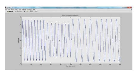
Figure 13. Generated waveform for given input Simout values
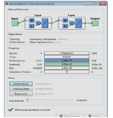
Figure 14. Neural network train tool
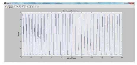
Figure 15. Neural Network output waveform after training
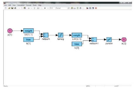
Figure 16. Feed Forward Neural Network FPGA Design flow
FPGA Implementation is done using the Xilinx ISE EDA tool. FPGA design involves writing HDL (hardware description language) code, creating test benches ( test environments), synthesis, implementation and debugging. A brief overview is as shown in Figure 17.
The simulation, synthesis and implementation will be discussed in this section. The verilog code developed for the neural network is simulated in VCS (Verilog Compiler Simulator). The simulation results of each layer of design using VCS is observed. The design is synthesized using Xilinx ISE and implemented on Virtex-5 FPGA board. RTL schematic and devise utilization of the design is obtained after synthesis process.
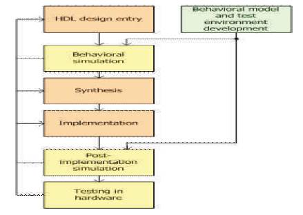
Figure 17. FPGA Design flow
The block diagram shown in Figure 18 is that of the designed Feed Forward Neural Network. It consists of an input which is given to the hidden layer. Hidden layer consists of Input weights and biases. The input values are multiplied to the weights and then the bias values are added to the product. This gives us a new output which is the total output of Hidden Layer. The output of the output layer is calculated in the same way as the hidden layer, but the bias b(2) is not added to it. This gives us the output of the output layer. The outputs of Hidden Layer and Output Layer are multiplied. This result is then added to bias b2 to get the final output of entire network. The verilog coding is done for this network and inputs are specified as parameters. The simulation results of each layer of design using Verilog Compiler Simulator (VCS) is observed. The design is synthesized using Xilinx ISE and implemented on Virtex-5 FPGA board. Register Transfer Level (RTL) schematic and devises utilization of the design is obtained after synthesis process.
The Feed Forward Network is designed for 50 inputs. The verilog code developed for this network experiences IO bound issues when implemented on FPGA. Hence the inputs and outputs are considerably reduced to implement the design.
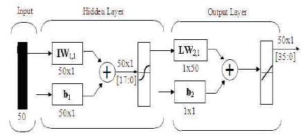
Figure 18. Block Diagram of designed Feed Forward Neural Network
Hidden layer as shown in Figure 19 consists of Input weights and biases. These weights and biases are obtained from the command window of matlab as coefficients of neural network. The input values are multiplied to the weights and then the bias values are added to the product. A new output is obtained which is the total output of Hidden Layer. The verilog coding is done for this network and inputs are specified as parameters. The simulation results of the Hidden Layer using VCS is observed.
Verilog code is developed for Hidden Layer. The Input weights and biases obtained are converted into 2's complement 9-bit binary numbers. The Input weights and biases are now declared as input parameters in the code. Initially four inputs will be given to Neural network algorithm. Any one of them is taken and multiplied with Input weights. A 9x9 Booth's Multiplier is used for multiplication. The multiplier outputs are then added altogether, which results in a single 18-bit value. This single value is added to every bias value b(1), which are also declared as input parameters. The addition is performed by a 18-bit adder which is triggered by the clock. This addition results in fifteen 18-bit values as the Hidden Layer outputs (t0-t14). The design is synthesized using Xilinx ISE and implemented on Virtex-5 FPGA board. RTL schematic as shown in Figure 20 is obtained after synthesis process.
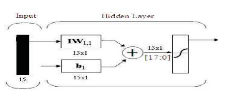
Figure 19. Hidden Layer
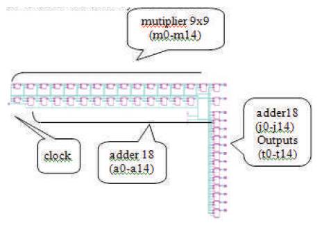
Figure 20. RTL schematic of Hidden Layer
Output layer as shown in Figure 21 consists of Layer weights and bias. These weights and biases are obtained from the command window of matlab as coefficients of neural network. The output of the output layer is calculated in the same way as the hidden layer but the bias b2 is not added to it immediately. This gives us the output of output layer. The verilog coding is done for this network and inputs are specified as parameters. The simulation results of Output layer using VCS is observed.
Verilog code is developed for Output Layer. The Layer weights obtained are converted into 2's complement 9- bit binary numbers. The Layer weights are now declared as input parameters in the code. Initially, four inputs will be given to Neural network algorithm. Any one of them is taken and multiplied by Input weights. A 9x9 Booth's Multiplier is used for multiplication. The multiplier outputs are then added altogether, which results in a single 18-bit value. The addition is performed by an adder which is triggered by the clock. This addition results in a single 18- bit value as the Output Layer output (outp2). The design is synthesized using Xilinx ISE and implemented on Virtex-5 FPGA board. RTL schematic as shown in Figure 22 is obtained after synthesis process.
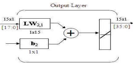
Figure 21. Output Layer
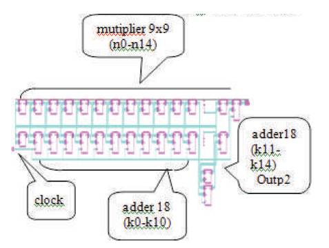
Figure 22. RTL schematic of Output Layer
The combination of both hidden layer and output layer forms the Top Module. The output of Top module is the final output (comout0-comout14). The Hidden Layer outputs (t0-t14) are multiplied with the Output Layer output (outp2). An 18x18 Booth's Multiplier is used for multiplication. This results in fifteen 36-bit values as outputs. These multiplier outputs are added to the single bias value, b(2). The addition is performed by a 36-bit adder which is triggered by the clock. This addition results in fifteen 36-bit values as the Hidden Layer outputs (comout0-comout14).
Virtex-5, the device required for FPGA implementation is interfaced with the computer via a JTAG USB port (Figure 25). The generated programming file is dumped into Virtex-5 via this JTAG USB port. Once the top module code is synthesized, its design is implemented on the specified device which is Virtex-1. Virtex-5 FPGA board is interfaced with the computer in which the top module code is synthesized and implemented. The Experimental Setup is as shown in Figure 23.
Once the interfacing is done, the corresponding programming file for the top module is generated. The target device is then configured so that the generated programming file can be successfully dumped on Virtex- 5 as shown in Figure 24. The design is then analyzed using Chip Scope Pro. The Chip Scope output is observed. The Chip Scope output is successfully compared with VCS simulation output.
Feed Forward Neural Network consists of Hidden layer and Output Layer. It consists of an input which is given to the hidden layer. Hidden layer consists of Input weights and biases. The input values are multiplied to the weights and then the bias values are added to the product. This gives us a new output which is the total output of Hidden Layer. The output of the output layer is calculated in the same way as the hidden layer, but the bias b(2) is not added to it. This gives us the output of the output layer. The outputs of Hidden Layer and Output Layer are multiplied. This result is then added to bias b2, to get the final output of the entire network. The verilog coding is done for this network and inputs are specified as parameters. The simulation results of each layer of design using Verilog Compiler Simulator (VCS) is observed. The design is synthesized using Xilinx ISE and implemented on Virtex-5 FPGA board
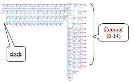
Figure 23. RTL schematic of Top module
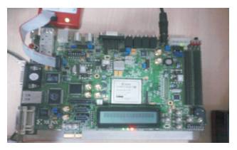
Figure 24. Virtex-5 FPGA board

Figure 25. FPGA implementation
Hidden layer consists of Input weights and biases. These weights and biases are obtained from the command window of matlab as coefficients of neural network. The input values are multiplied to the weights and then the bias values are added to the product. This gives us a new output which is the total output of Hidden Layer. The verilog coding is done for this network and inputs are specified as parameters. The simulation results of design using VCS is as shown in Figure 26. The Xilinx ChipScope tools are added to the Verilog design to capture input and output directly from the FPGA hardware. The design is again synthesized using Xilinx ISE and implemented on Virtex-5 FPGA board. The hidden layer simulation in ChipScop pro is shown in Figure 27.
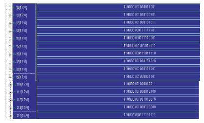
Figure 26. Hidden Layer simulation in VCS
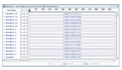
Figure 27. Hidden Layer simulation in ChipScope pro
Output layer consists of Layer weights and bias. These weights and biases are obtained from the command window of matlab as coefficients of neural network. The output of the output layer is calculated in the same way as the hidden layer but the bias b2 is not added to it immediately. This gives us the output of the output layer. The verilog coding is done for this network and inputs are specified as parameters. The simulation results of each output layer of design using VCS is as shown in Figure 28. The Xilinx ChipScope tools are added to the Verilog design to capture input and output directly from the FPGA hardware. The design is again synthesized using Xilinx ISE and implemented on Virtex-5 FPGA board. The output layer simulation in ChipScope pro as shown in Figure 29.
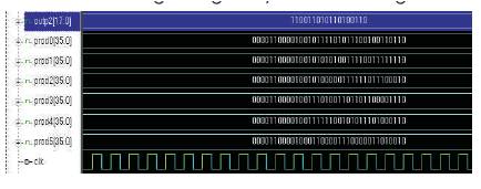
Figure 28. Output Layer simulation in VCS
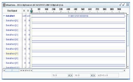
Figure 29. Output Layer simulation in ChipScope pro
This is the complete combination of both hidden layer and output layer. The output of this Top module is the final output. The verilog coding is done for this network and inputs are specified as parameters. The simulation result using VCS in top module is as shown in Figure 29. The Xilinx ChipScope tools are added to the Verilog design to capture input and output directly from the FPGA hardware. The design is again synthesized using Xilinx ISE and implemented on Virtex-5 FPGA board. The top module simulation in ChipScope is as shown in Figure 30.
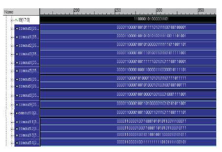
Figure 30. Top Module simulation in VCS
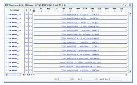
Figure 31. Top Module simulation in ChipScope pro
Selected Device: 5vlx110tff1136-1
Slice Logic Utilization:
Number of Slice LUTs: 4666 out of 69120 6%
Number used as Logic: 4666 out of 69120 6%
IO Utilization:
Number of IOs: 558
Number of bonded IOBs: 558 out of 640 87%
IOB Flip Flops/Latches: 15
Number of BUFG/BUFGCTRLs: 1 out of 32 3%
Minimum input arrival time before clock: 25.682ns
Maximum output required time after clock: 3.524ns
Maximum combinational path delay: 28.470ns
Total quiescent power: 0.97905 W
Total Dynamic power: 0.03580 W
Total Power: 1.01485 W
The simulation results of the hardware model for each sub block of the neural network are obtained. The simulations are performed in VCS. The functionality of hardware models are cross verified with that of the results obtained from Chip Scope Pro. The design is optimized for power of 1.01485 W and memory of 540916 kilobytes.
Simulink block of ANN based Image Compression unit is designed using the MATLAB. Multiple signals are given to check the performance of filters. Frequency domain and Time domain responses are checked in Spectrum scope and scope respectively. Simout values of individual signals are determined. These values are then given as input to Neural Network Algorithm, developed in Matlab, for training. The Feed Forward Neural Network is generated. The coefficients of this network are obtained from the Matlab command window. The coefficients obtained are Input weights (IW), Layer weights (LW) and biases b(1) & b(2). A verilog code is developed for the network and is implemented on FPGA. The Input weights (IW), Layer weights (LW) and biases b(1) & b(2) are given as parameter inputs in the verilog code. Verilog code of the model is developed for simulation on the VCS (Verilog Compiler Simulator). The simulation results of this code are checked and compared with that of Chip Scope results obtained as a result of FPGA implementation.
The FPGA implementation is carried out using Xilinx ISE 10.1. The implementation is performed on Virtex-5 FPGA board. Once the interfacing is done, the corresponding programming file for the top module is generated. The target device is then configured so that the generated programming file can be successfully dumped on Virtex- 5. The design is then analyzed using Chip Scope Pro. The Chip Scope output is observed. The Chip Scope output is successfully compared with VCS simulation output. The design is optimized for power of 1.01485 W and memory 540916 Kb. The RTL model can also be implemented on ASIC.