(1)
As the dimension of interconnects in Integrated circuits has become dominant, the inductive effects of the wires cannot be ignored anymore. At high frequency, the return current distributes itself close to the signal path and any increase in the inductance of the return path hampers signal integrity. The multi-layered Power Distribution Network (PDN) is stressed when many devices draw current simultaneously, creating noise in the supply rails. This high speed current not only causes ground bounce and power supply sag but it also needs a low inductance return path. Since high frequency involved in contemporary signaling makes the interconnects to behave as lossy transmission lines, the chip may sustain less noise margin due to environmental or process variations. If the inductive effort is considered, the design will be more robust and variability-free, thus improving the defect tolerance. In this paper, a SPICE based analysis of “on-board” high speed return current path is conducted and techniques and results are then extended for “on-chip” return current path analysis. In addition to avoiding operational failures, a priori knowledge of signal and its respective return path would greatly help to simplify interconnect designing and routing.
As the operating frequencies continue to rise in contemporary integrated circuits, inductive effects of interconnects must be included in the designing process. These inductive effects create noise in the power distribution network, ringing, overshoot/undershoot and reflection problems. Due to inductance being a loop phenomenon, the distribution and path of return currents must be known in order to avoid signal integrity problems. At high frequencies, in order to minimize the loop inductance, the return currents are confined to the nearest reference plane and follow the signal current closely. Any discontinuity in the return path causes the inductance to grow and results in the degradation of the signal. These discontinuities might be caused due to various reasons such as vias on the signal trace or high speed signal crossing multiple voltage reference planes on the same layer. In this paper the authors simulated the path of return currents on solid and split reference planes and obtained useful results for the distribution of return currents on a printed circuit board. The same observations can be applied to “on-chip” return current analysis. Some constructive effects of the inductance such as improved transition time and reduced dynamic power consumption [9] are also highlighted.
The rest of the paper is as follows: related research work is presented in section 1, section 2 presents the theory, section 3 contains the details of the experiment, section 4 explains the transmission line model, section 5 describes on-chip inductance, section 6 presents the result and the last is the conclusion of the paper.
There has been much research into the inductive properties interconnects both on-board and on-chip. Arora et al. [1] reviewed different approaches to model the onchip wire inductance and discussed methods to assess the inductance with special reference to return current path. Research in [2] presented an efficient performance optimization technique for distributed RLC interconnects and illustrated the implications of technology scaling on wire inductance. Signal integrity aware design techniques and the inductive property of the interconnect are presented in [3]. Cao et al. [4] discussed a numerical approach to model the effective loop inductance for multiple lines considering static timing analysis. The work in [5] analyzed the results of inductive effects on signal nets for ultra-deep submicron technologies under the influence of power grid noise and the impact of on-chip inductance from Al and Cu based interconnects.
Das et al. [6] proposed the concept of an optimal inductance value that can substantially reduce delay of global RLC signals. The work accomplished in [7] described the impact of on-chip inductance on power supply integrity. Fan [8] presented the process variation-aware interconnect simulation and optimization in VLSI designs. The undesirable effects of on-chip inductance like higher interconnect coupling noise and challenges for accurate extraction as well as some desirable effects such as lower power consumption, less need for repeaters and faster signal rise time are covered in [9]. Ismail et al. [10, 11] described the effects of on-chip inductance on clock distribution networks and RLC trees.
The distribution of return current in a printed circuit board and the effects of added inductance of return path on signal integrity are emphasized in [12]. Leferink et al. [13] discussed the Inductance of printed circuit board ground planes. The impact of on-chip inductance and the properties of on-chip current loops are covered in [14,15]. Research work in [16] presented various power distribution networks and the effects of decoupling capacitance on power grid noise. Qi et al. [17] described techniques to model the inductance of on-chip interconnects and compared the simulation results with measured data. The flow of signal on a lossy and loseless transmission line is presented in[18]. Study in [19] described the measurement of on-chip transmission line effects in a 400 MHz processor. Smith et al. [20] used RLC and transmission line elements to model a power plane in SPICE simulation program and simulated performance for different materials and geometries. Srivastava, Qi and Banerjee [21] presented the impact of Inductance on power distribution network design for nanoscale integrated circuits. This paper analyzes the printed circuit board return current distribution and its effects on signal integrity and extends it to cover the onchip interconnects.
Current always flow in loops and return back to the point of its origin taking the path of least impedance. At DC or very low frequencies, the return current distributes itself over the path having the least resistance [12]. This return path is generally the whole reference plane nearest to the signal current. The path taken by return currents in the case of low frequencies is presented in Figure 1. Observed in the figure, the signal current is flowing out of the driver over the bold trace and the return current (dotted line) is distributed all across the reference plane.
As we move towards higher frequency of operation, the characteristics of the return current changes significantly. At higher frequencies, inductance becomes more dominant than the resistance and the return current flows through the path of least inductance [12] as shown in Figure 2. The magnetic fields produced around a conductor when a current is flowing through it contribute towards self inductance. When the magnetic flux lines of one conductor interact with another conductor nearby, mutual inductance is created. A visual representation of self and mutual inductance is presented in Figure 3.
In Figure 4, conductor A carries the signal current and conductor B carries the return current. The total loop inductance is given by [3]:
Where,
Lloop= the loop self-inductance
La= self-inductance of leg a
Lb= self-inductance of leg b
Lab= mutual inductance between legs a and b
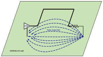
Figure 1. Low frequency return current path
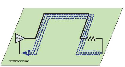
Figure 2. High frequency return current path
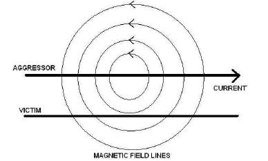
Figure 3. Magnetic field lines
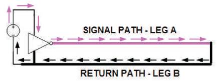
Figure 4. Signal and return current path
Very useful results can be extracted from equation (1) to minimize the total loop inductance. Firstly, the self inductances must be kept small. This can be achieved by using wider conductors or solid planes as reference. Secondly, in order to increase the mutual inductance, conductors A and B must be placed close to each other. This is achieved by putting the signal and its respective return path in close proximity. Highest mutual inductance is created when the return current is flowing exactly beneath the signal current. Figure 5 shows the return current density in a PCB cross section[12]. H is the dielectric thickness and D is the distance from the center of the trace.
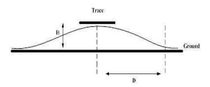
Figure 5. Return current density
A return plane can be thought as a network of a large number of resistors, capacitors, and inductors in a “springbed” architecture as shown in Figure 6 [20]. The circuit in the figure is the basic building block “Unit Cell” of the reference plane model. The unit cells can be arranged in an array structure to represent a model of a reference plane as shown in Figure 7. To model the high frequency return path, the author will inject a current from one unit cell and then receive the current from the cell on the opposite side. The idea behind this approach is to model the return current of a high speed signal flowing in a trace just above the reference plane. As we know from knowledge of previous sections at high frequencies, the return current flows through the path of least inductance which will be concentrated under the signal path.
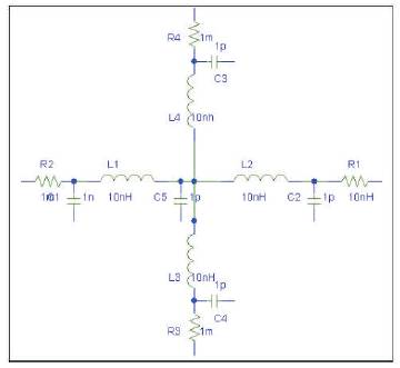
Figure 6. RLC unit cell
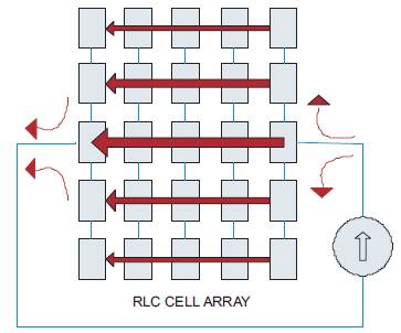
Figure 7. Return plane model
Earlier in this section the researchers discussed the properties of the return plane and how it could be modeled. We have to consider two variants of the return plane, namely
Solid reference plane refers to a continuous path for return currents. The return currents closely follow the signal current in this case and we get the best signal quality over the net. Figure 4 shows the structure of a solid plane. As we can see, the return current will flow back to source in an unrestricted manner. For the simulation of the solid reference plane we use the network implementation shown in Figure 10 with an 11 by 11 matrix.
3.1.2 Split Reference PlaneAs our designs are growing larger every day, it becomes necessary to split the layer of a PCB in order to accommodate multiple reference planes at the same level. This presents a serious hazard for return currents as they encounter a discontinuity in their path. As we know that the current must flow in a loop, it searches for an alternative path to return back to the source. This diversion causes the total loop inductance to grow in the return path and distorts the signal integrity. As an illustration, Figure 8 presents this scenario. We can see that the return current jumps from the 3.3 V plane to the 5 V plane and then to the ground plane in search of an alternative path towards the source. For the simulation of the split reference plane we will use the network implementation shown in Figure 9. Figure 9 shows that for modeling a split in the reference plane, we can remove the unit cells from the center of the network and keep the two cells at the two edges of the network intact in order to provide a conducting medium for the return current to flow. Figure 11 shows the plot for split plane.
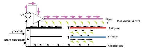
Figure 8. Split reference plane schematic
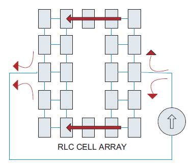
Figure 9. Split reference plane model
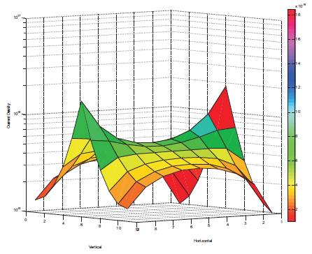
Figure 10 Solid reference plane MATLAB plot
As we now know, an ideal plane has an uninterrupted path for the return current to flow back to its source. Thus, it can be modeled as shown in Figure 12. Also, since the non ideal reference plane introduces extra inductance in the return path, it can be modeled as shown in Figure 13. The value of the inductor is varied as to simulate the different lengths of splits on the plane.
Figure 14 shows the simulation results for the two circuits. It is evident from the figure that the ideal reference plane (L=0 nH) is the best path for the return current. Increasing the inductance to 20nH, 60nH and 100nH considerably degrades the signal.
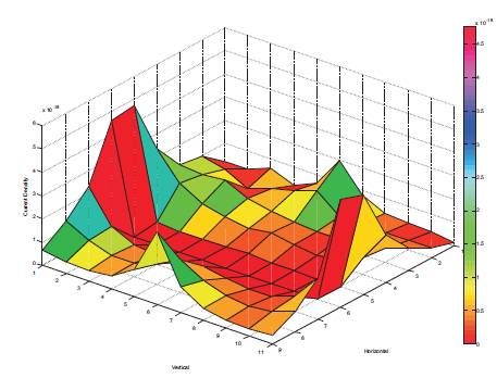
Figure 11. Split reference plane MATLAB plot
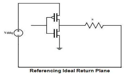
Figure 12. Simulation model for solid reference plane
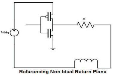
Figure 13. Simulation model for split reference plane
Figure 14. Simulation results for split reference plane
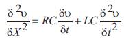
Due to the wavelengths involved in today's signaling, a lumped RC model does not suffice and a distributed RLC model must be used to better predict the behavior of the interconnects. On a transmission line, a signal propagates as a wave by alternatively transferring energy from the electric to the magnetic field [18].
Where,
C = capacitance
L = Inductance
R = Resistance
ν = voltage
X = position along the transmission line
t = time
The wave propagation equation for a transmission line is given by equation (2) with an assumption of conductance G=0. An interconnect can be represented as either a loseless or lossy transmission line based on its RLC properties. At the on-board level, due to the high conductivity and increased width of the trace, the resistance does not play a dominant part and for simplifications only the L and C components can be considered [18]. This model is referred to as the loseless transmission line model, as shown in Figure 15.
Where,
C = capacitance
L = Inductance
ν = voltage
X = position along the transmission line
t = time
Equation (3) gives the mathematical representation of a loseless transmission line. On the other hand, due to the shrunken width of the on-chip interconnect, the resistance cannot be ignored and a lossy transmission line model must be adopted, as shown in Figure 16. Lossy RLC model encompasses both the wave propagation and diffusive components. Thus, the unit cell model used for on-board return current path modeling can be extended to cover the on-chip analysis.
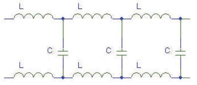
Figure 15. Loseless transmission line model
As pointed out before, a significant amount of noise is created in the power distribution network because of the inductive properties of the wire. Figure 17 represents such a situation. When the device is switching, it (dis)charges the load capacitance. A current flowing to (dis)charge the load capacitance passes through the parasitic inductance of the power distribution network and changes the value of the reference voltages available to the device. In this case, the value of Vdd is reduced to Vdd' and GND is increased to GND' resulting in less noise margin. This phenomenon is termed as power supply sag or ground bounce and it directly contributes to jitter. The situation becomes even worse when many devices share the common supply pin and switch simultaneously. The performance of the IC is directly dependent upon the voltage available to the devices and thus a large fluctuation in the power distribution network can also result in timing violation.
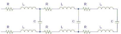
Figure 16. Lossy transmission line model
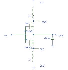
Figure 17. Voltage supply sag/ ground bounce
In contrast to the printed circuit board, where the dimensions of the interconnect are virtually constant, the on-chip interconnect hierarchy differs drastically [18]. Onchip wires are divided into global and local wires as shown in Figure 18 which presents the interconnect hierarchy for a 0.25um CMOS process. Global wires are designed to keep the resistance small whereas the local wires are shrunk to accommodate high integration density and have less capacitance which is crucial for high speed operation. In Figure 18, M6 and M5 represent the higher metal layers which are used to distribute power and ground reference. As we move down, the wires keep shrinking and the density increases. Different dimensions of the interconnect layers causes different values of the inductive component which adds up since the loop of the current starts from higher metal layers and goes back.
An in-depth analysis of on-chip inductance has been covered in[1-2, 4-7, 9-21]. The positive effects of on-chip inductance on signal transition time, repeater insertion process, power dissipation, and delay uncertainty are investigated in [9]. The return current path is intuitive during PCB routing and a well designed printed circuit board is considerably immune to the inductive effects. In the onchip regime, inductance extraction becomes a major challenge[1, 6, 7, 15, 21]. Densely packed interconnect structures and substrate coupling makes it difficult to predict the return path in advance.
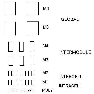
Figure 18. Interconnect Hierarchy 0.25um CMOS process (Not drawn to scale)
On-chip power distribution network design needs special attention[16]. Every device must get sufficient voltage in order to operate as intended. As described in the previous sections, the larger the current loop, the greater the signal degradation. Power noise can result in jitter[18], so a thorough analysis of return current path of global signals like clock and high speed buses must be performed before making the timing budget. Simulations must be carried out by varying the inductance as shown previously to get the value of allowable degradation. The network then should be designed to match and minimize the return current path.
SPICE netlist for the solid and split reference plane were simulated and results are plotted using MATLAB. presents the plot for the solid plane. As expected, a Gaussian distribution is obtained. Density of the current is more in the center and fades down as we move away.
Figure 11 presents the plot for the split plane. As we can see, the return current encounters a discontinuity and searches for an alternative path with minimum inductance towards the source. This distribution shows the extra inductance encountered when the return current takes an alterative path. The introduction of extra inductance in the return path considerably degrades the signal integrity.
Interconnect inductance has become a dominant problem in contemporary designs. High speed signals suffer degradation due to the inductive effects caused by the return current path variations. We have modeled the effects of discontinuities in the current return path and presented its effects on signal quality. The simulations and results can be applied to the on-chip counter-part. Treating the interconnect as an RLC network gives us more control over our designs. Including inductance in our analysis also results in savings in terms of power dissipation, signal transition time, repeater insertion, and delay uncertainty. Reduced number of devices and simplified routing will result in more defect tolerance. Return current path based inductance analysis is thus a very useful tool for making robust high speed designs.