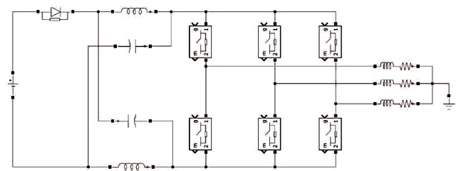
Figure 1. Z-Source Inverter Circuit Topology
The impedance-source power converter (Z-Source inverter) has become progressively well known and is considered as a unique alternative for classic inverters. Z-Source inverter advantageously eliminates the conceptual and theoretical limitations of conventional inverters and provides an advanced power conversion concept, which is not conceivable in Voltage Source Inverter (VSI) and Current Source Inverter (CSI). It has a particular impedance network, where a capacitor and inductor are combined into the Z network to link the inverter circuit to the DC power source. Classic carrier-based Pulse Width Modulation (PWM) control techniques of the Z-Source inverter are simple boost control, maximum boost control and maximum constant boost control respectively. In this paper, a comparative analysis of three different control techniques of the Z-Source inverter for the determined boost factor (B) is conducted based on simulations and mathematical analysis using MATLAB/Simulink. Maximum voltage stress applied on semiconductor devices (Vs), voltage gain (G) and modulation index (M) of each control techniques are compared in details. According to the obtained results Maximum Boost Control techniques has better performance than other PWM control techniques.
Today power inverters are mainly used in many fields including renewable energy systems, AC motor control, uninterruptied power supplies, induction heating and variable speed drives. According to their working principle and type of utilized power source, conventional inverters can be classified as VSI and CSI. Both inverter types have their own disadvantages, such as two stage power conversion, effect of electromagnetic interference, dead time obligation between the switches in the same leg and more harmonics in output voltages (Endiz et al., 2016; Wang et al., 2009). In order to eliminate the disadvantages of conventional VSI and CSI, Z-Source inverter circuit topology has been introduced as shown in Figure 1 (Peng, 2003). Z-Source inverter has a particular impedance network, which is composed of two inductors (L1 and L2) and two capacitors (C1 and C2) combined in Z- network to link the inverter circuit to the DC power source (Peng, 2003; Endiz & Akkaya, 2018; Liu et al., 2016). In Z- Source inverter both of the power devices in the same leg can be switched ON at the same time that eliminates dead time. Therefore, the reliability is significantly improved and the output waveform distortion is considerably reduced. Z-network does not need a transformer or a DC-DC converter circuit. The boosting process is based on short-circuit operation of the inverter legs, making it resistant to electromagnetic interference that cannot be observed in the VSI and CSI. Since Z-Source inverters overcome all these drawbacks, they have emerged as a less complex and cost-effective circuit structure with a single-stage power converter (Peng et al., 2005a; Peng et al., 2003). The main goal of this paper is to conduct a comparative analysis of three different control techniques of the Z-Source inverter for a determined boost factor.
Figure 1. Z-Source Inverter Circuit Topology
In this paper, simulations of three different control techniques of the Z-Source inverter used MATLAB/Simulink program, which is widely utilized in academic studies and applications in many engineering fields. Working in the MATLAB/Simulink environment allows researchers flexibility in design and the ability to easily apply dynamic parameter values in many cases, which gives the work reliability.
There are various modified PWM control techniques for the Z-Source inverter based on classic PWM control methods. Classic carrier-based PWM control techniques of the ZSource inverter are simple boost control, maximum boost control and maximum constant boost control respectively (Peng, 2003).
Voltage gain and total harmonic distortion at different modulation indexes of different control methods are presented by Nayak and Dash (2012). Four different shootthrough control methods are presented in terms of the voltage and current harmonic, the DC link voltage ripples, the switch voltage stress, the inductor current ripples, the output voltage and the efficiency by Ellabban et al. (2011). Modified space vector pulse width modulation method and the simple boost control methods are compared in terms of the harmonics, the total average and peak switching device power by Pham et al. (2012). The relationship between the PWM inverters and Z-Source inverters, their various control methods, and the dead time effect on harmonics are discussed by Abu-Rub et al. (2012).
Simple boost control technique is the first control technique of Z-Source inverter (Peng, 2003). The control signals and shoot-through pulses used in simple boost control are demonstrated in Figure 2 and Figure 3 respectively. In the simple boost control technique, two straight envelope lines that are equal to or greater than the maximum value of the three phase references, set the shoot-through duty ratio. The inverter is turned into a shootthrough state, when the carrier triangle wave is greater than the upper shoot-through envelope or smaller than the lower shoot-through envelope (Vp and Vn). The inverter switches meanwhile in the same way as the classic carrierbased PWM control.
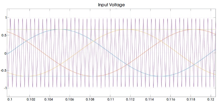
Figure 2. Control Signals of the Simple Boost Control Technique
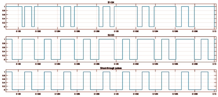
Figure 3. Shoot-Through Pulses used in Simple Boost Control
The related equations of the simple boost control technique are given below:


where, T is the switching period, Tkd is the shoot-through time, Ts is the non-shoot-through time, D is the short circuit duty ratio, B is the boost factor, G is the voltage gain, M is the modulation index and Vs is the maximum voltage stress applied to the semiconductor devices.
The operating principle of the maximum boost control technique is similar to the classic carrier-based PWM control method (Peng et al., 2005b). The control signals and shoot-through pulses used in maximum boost control are demonstrated in Figure 4 and Figure 5 respectively. This technique performs unchanged six active states, turning all zero states into shoot-through states. Thus the maximum shoot-through time and boosting factor are achieved for any specified modulation index without affecting the output waveforms. The circuit is in shoot-through state, when the triangular carrier wave is either greater than the maximum reference curve or smaller than the minimum reference curve (Va, Vb, Vc).
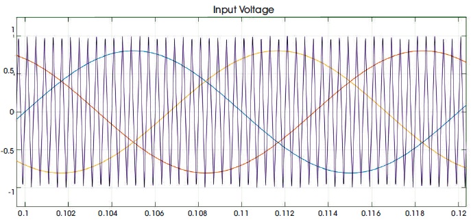
Figure 4. Control Signals of the Maximum Boost Control Technique
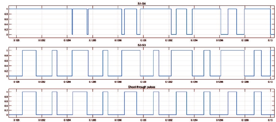
Figure 5. Shoot-Through Pulses Used in Maximum Boost Control
The related equations of the maximum boost control technique are given in Equations (6), (7) and (8):


Maximum constant boost control technique can significantly decrease the L and C requirements of Z networks (Shen et al., 2004). The control signals and shoot-through pulses used in maximum boost control are demonstrated in Figure 6 and Figure 7 respectively. Maximum constant boost control technique keeps the duty ratio of the shoot-through constant, while achieving the maximum voltage gain. This technique contains five modulation curves: three reference signals Va, Vb, Vc, and two shoot-through envelope signals Vp and Vn. The inverter is turned into a shoot-through state, when the carrier triangle wave is greater than the upper shoot-through envelope Vp or smaller than the lower shoot-through envelope Vn.
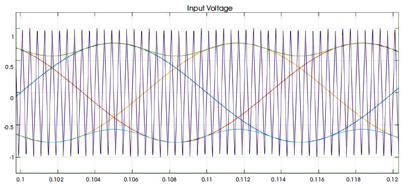
Figure 6. Control Signals of the Maximum Constant Boost Control Technique
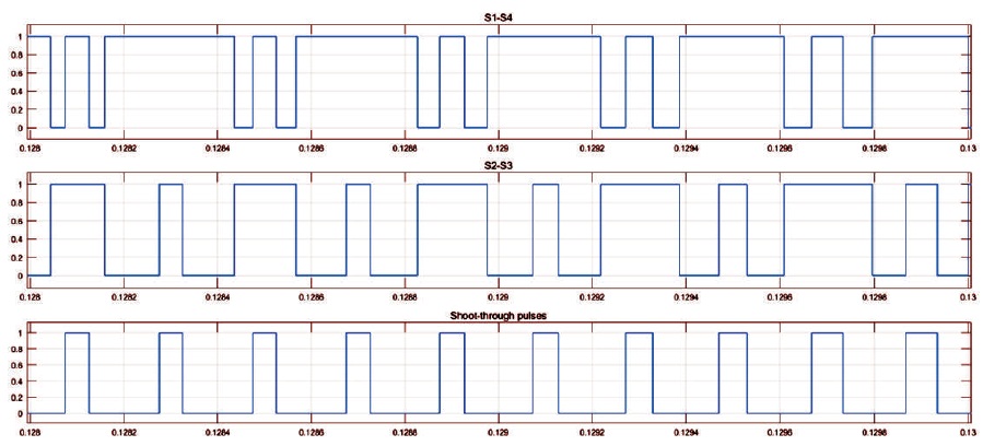
Figure 7. Shoot-Through Pulses Used in Maximum Constant Boost Control
The related equations of the maximum constant boost control technique are given in Equations (9), (10) and (11):


Simulations and mathematical analysis of three different control techniques of the Z-Source inverter discussed in this paper are performed separately and the results are given in the following figures. Maximum voltage stress applied on semiconductor devices (Vs), voltage gain (G), and modulation index (M) are analyzed in details and compared using MATLAB/Simulink for a determined boost factor B = 3.3. For the simulations the selected parameters are as follows: The input DC voltage Vg = 150 V, inductors and capacitors of the Z-Source L1 = L2 = 160 μF, C1 = C2 = 1000 μF respectively, switching frequency of the semiconductor devices fs = 10 KHz and load R = 50 ohm. The equation of the modulation index, which is characterized as the ratio of the peak value of reference wave to the peak value of the carrier wave is given in equation (12). Under modulation index for M<1, the relationship between modulation index and output voltage is generated.

Using simple boost control the maximum voltage stress applied on semiconductor devices (Vs) increases to 550 V and the output peak phase voltage (Vphase) after the low pass LC filter is about 200 V according to the Figure 8 and Figure 9. Mathematical analysis for simple boost control are calculated below.
Vs = B*Vg = 3.3*150 = 495V
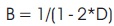
B = 1/(1-2*D) = 1/(2* M-1) and B = 3.3 therefore M = 0.651
G = M*B = 2.15
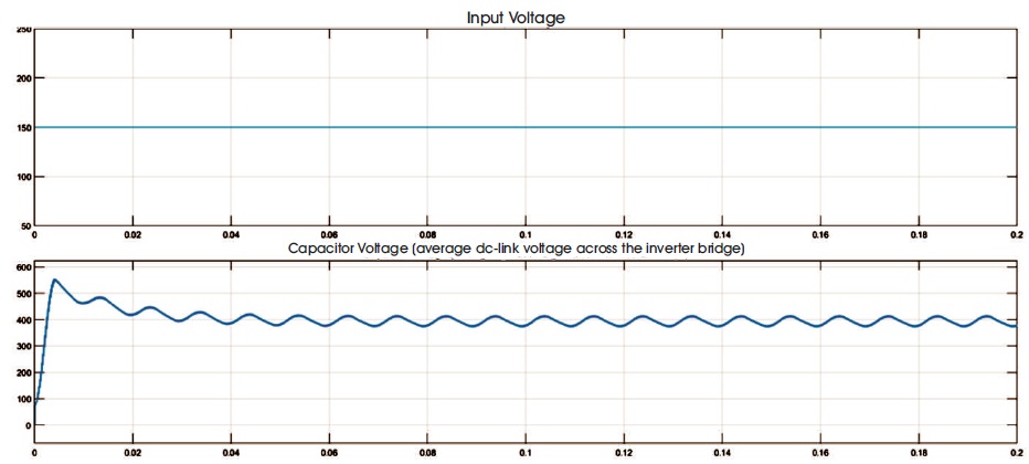
Figure 8. Maximum Voltage Stress on Semiconductor Devices
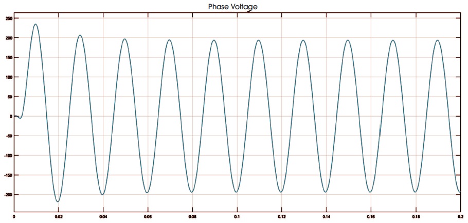
Figure 9. Output Peak Phase Voltage After the Low Pass LC Filter
Using maximum boost control the maximum voltage stress applied on semiconductor devices (Vs) increases to 515 V and the output peak phase voltage (Vphase) after the low pass LC filter is about 250 V according to the Figure 10 and Figure 11. Mathematical analysis for maximum boost control are calculated below.
Vs = B*V = 3.3*150 = 495V
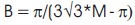
B = π/(3√3*M -π) and B = 3.3 therefore M = 0.807
G = M*B = 2.66
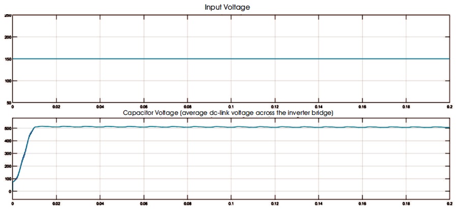
Figure 10. Maximum Voltage Stress on Semiconductor Devices
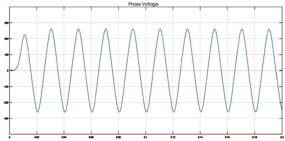
Figure 11. Output Peak Phase Voltage After the Low Pass LC Filter
Using maximum constant boost control the maximum voltage stress applied on semiconductor devices (Vs) increases to 495 V and the output peak phase voltage (Vphase) after the low pass LC filter is about 230 V according to the Figure 12 and Figure 13. Mathematical analysis for maximum constant boost control are calculated below.
Vs = B*V = 3.3*150 = 495V
B = 1/(3√3*M-1) and B = 3.3 therefore M = 0.751
G = M*B = 2.48
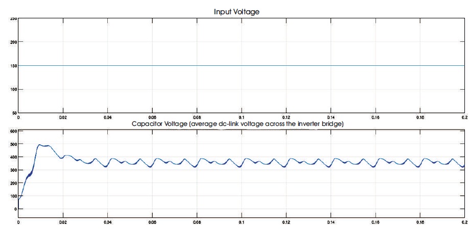
Figure 12. Maximum Voltage Stress on Semiconductor Devices
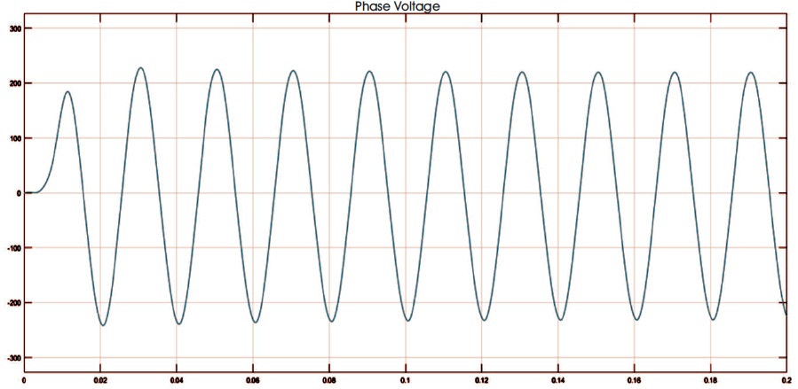
Figure 13. Output Peak Phase Voltage after the Low Pass LC Filter
The correlation between the maximum voltage stress applied on semiconductor devices, voltage gain and modulation index is given in Table 1. As indicated in Table 1, while the maximum boost control has the largest modulation index and therefore has the highest voltage gain, maximum constant boost control has the lowest voltage stress applied on semiconductor devices. Simple boost control can easily be used for applications where higher voltage gain is not demanded. According to the Figure 8 to Figure 13, simulation results and mathematical analysis differ slightly from each other in terms of maximum voltage stress applied on semiconductor devices due to the MATLAB/Simulink environment.
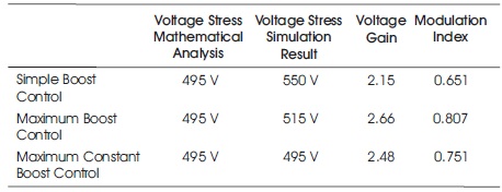
Table 1. Comparative Analysis of Z-Source Inverter Control Techniques for B = 3.3
Figure 13. Output Peak Phase Voltage after the Low Pass LC Filter
Based on the research objective of this paper, we have come to the following results. As a result of the performed simulations and mathematical analysis among the various control techniques, the maximum boost control has the largest modulation index and therefore has the highest voltage gain for the Z-Source inverter. The main problem of the maximum boost control is the increase in inductance size due to the change of the shoot-through duty ratio. This could increase the total cost of the system. In the maximum constant boost control maximum voltage stress applied on semiconductor devices is the lowest and is mostly preferred in high-power applications, because high voltages on semiconductor devices lead to switching losses that are direct effect on system efficiency and reliability. Simple boost control is frequently used for low-power applications such as microinverter applications where the supply voltage is sufficient and higher voltage gain is not required. However, the main drawback of this technique is the maximum voltage stress applied on semiconductor devices is the highest, which necessitates the limitation of high voltage ratings of switches. Therefore this technique cannot be used to get higher gain due to the causing of the cost increase.
In this paper simulation and mathematical analysis of three different control techniques of the Z-Source inverter for a determined boost factor is carried out with the same input voltage and load conditions. The simulation results for three different control techniques mostly match the theoretical analysis. From the results obtained, maximum boost control is the most preferable control techniques, which is the best option for Z-Source inverter, because of its high voltage gain and low voltage stress applied on semiconductor devices. All these three different control techniques of the Z-Source inverter can be utilized for industrial drives and other converter applications. Considering the high expectation on photovoltaic systems, converting the generated DC power into AC power with maximum efficiency and keeping losses at minimum level would be optimum. The study conducted in this paper will be an advisory research topic to get better results for future works.
Authors of this paper acknowledge the Department of Electrical and Electronics Engineering of Konya Technical University for providing technical support.