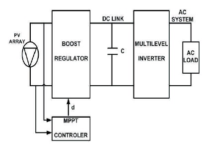
Figure 1. Schematic Block Presentation of Proposed System
The present work deals with five level reduced device count multilevel inverter topology for a single-phase standalone solar photovoltaic based power generation system. The essential switching design presented here is used to reduce the selective lower order harmonics from the output voltage. The DC-DC voltage regulator is used to obtain stable DC output from standalone solar photovoltaic system for which the Perturb and Observe algorithm has been used to obtain maximum power operating point technique (MPPT). The complete control technique has been explained with the help of different modes of operation for five level output voltage with only six Insulated Gate Bipolar Transistor and two diodes to extract maximum amount of solar photovoltaic energy to increase fundamental output voltage with minimum harmonic contents. The performance of presented system has been simulated and tested in MATLAB simulation environment. The analysis of harmonic content in the output voltage and current has been carried out for the system under test.
In the present scenario, nonconventional energy sources play a vital role in the field of power generation. Numerous non-conventional sources like; solar Photovoltaic (PV) system, geothermal and wind energy are suitable for electric power generation with more environmental friendly alternatives and are capable to capture the maximum energy from the non conventional energy source. The huge amount of solar energy reached to the earth from the sun is sufficient to supply electrical energy consumed annually by the entire world in a short interval of time, i.e. in half an hour. Depending on the latitude of location, the solar radiation on the surface of the earth is about 1000 watts per square meter. The sun is a largest clean non conventional energy source, which neither produces green house effect nor nitrogen waste through its consumption.
The solar PV system has no moving elements; it is totally a solid state and self-contained system. The solar PV array based power generation is desirable non conventional energy resource for financial development of countries. At present, solar PV array system as well as wind energy are the most explored technologies due to their considerable advantages in comparison to other non conventional energy resources (Sera, Teodorescu, Hantschel, & Knoll, 2008). Therefore, they have less impact on environment and their connection to grid system among all other power generating sources is very easy. Now a day's, solar power is one of the most reliable and environmental friendly technology and due to this it is mostly adopted worldwide. One day, the Solar PV system may replace the fossil fuel because it is environmental friendly and simple among all other non conventional energy sources. Other than this, the cost/kWh of solar PV system is less than fossil fuel based energy sources (Gules, Pacheco, Hey, & Imhoff, 2008).
Further, there are so many factors due to which the efficiency of solar PV system is less, such as; solar panel temperature and partial shading conditions, etc. In order to achieve maximum output power, it is essential to drive the solar PV array system at its maximum power operating point condition. It is achieved by implementing charge controllers along with maximum power operating point technique (MPPT). (Femia, Petrone, Spagnuolo, & Vitelli, 2009; Chiu, 2010).
For stand-alone solar PV array system, the main stream of predictable approach now a days is multilevel inverter topology due to its practicability and ease of implementation at diverse location to maintain high efficiency even when partial shading condition arise (Sokal, 1973). Solar PV array system is basically a non-linear type of power source and it depends on solar panel irradiation, solar panel temperature and type of load conditions; therefore MPPT is implemented to solar PV array system for achieving maximum output power at dissimilar location (Xiao, Ozog, & Dunford, 2007; Patel & Agarwal, 2009).
A properly designed solar PV array system with proper MPPT tracking system may easily recognized a point at which maximum power may obtain and increase the efficiency of the solar PV array system. In a complete system, the inverter plays a very important role in solar PV array system because it generates AC power from available DC source. The main drawback of conventional two-level inverter when it is used in solar PV array system is that it produces a large amount of harmonics and therefore triggering losses become high and produce a huge dVpv /dt stress across triggering devices (Aboadla et al., 2016). So, to minimize these types of problems multilevel inverters have been introduced in place of conventional two-level inverters (Rahim & Selvaraj, 2010; Ohsato, Kimura, & Shioya, 1991). Other than these, in multilevel inverters, there is a limitation of power switches, as the output voltage levels increase; the number of power switches also increase. In the prescribed work of reduced device count, multilevel inverters are implemented with a solar PV array system where total number of power switches was reduced and therefore triggering stress across the power devices as well as harmonic effect appear at the output of inverter also reduced (Massoud, Finney, & Williams, 2003).
The complete schematic block representation of proposed system is shown in Figure 1. A schematic block contains solar PV array system, boost regulator, DC Link (filters), DC-AC multilevel inverter and control logic for MPPT. Following sections describe each block in detail.
Figure 1. Schematic Block Presentation of Proposed System
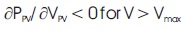
The major concept of the designed system is to obtain and control maximum power operating point, as shown in Figure 2 which is based on the fact that if əPPV/ əVPV = 0, the output power of solar PV array will be maximum as mentioned in equation (1). If the derivative is greater than zero, i.e. əPPV/ əVPV > 0, it deviates maximum power operating point towards left side region of the P-V curve mentioned in equation (2) and if it is less than zero, i.e. əPPV/ əVPV< 0, it deviates maximum power operating point towards right side region of the P-V curve mentioned in equation (3), respectively.
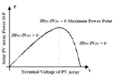
Figure 2. P-V Characteristics of Photovoltaic Cell
Several MPPT algorithms are now available to enhance the overall output efficiency and performance of solar PV system such as; Perturbs & Observes (P&O) algorithm, Parasitic Capacitance algorithm, Constant Voltage (CV) algorithm and Incremental Conductance algorithm, etc. However, the most widely used and accepted MPPT algorithm is P & O algorithm. The MPPT algorithm has been implemented at DC-DC Boost regulator gate side. The logic is designed according to the flow chart of P&O algorithm for direct triggering pulse cycle control of boost regulator output (Forouzesh, Siwakoti, Gorji, Blaabjerg, & Lehman, 2017). The value of this triggering pulse cycle lies in between 0 and 1. As the solar PV array voltage Vpv vary, there is a variation in the solar PV array power Ppv also, therefore triggering pulse cycle of the regulator is also changed as described by following simple logic;
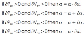
where, ə = triggering pulse cycle and əa is perturbation
DC-DC boost regulator is an integral part of any MPPT system. Without DC-DC boost regulator no MPPT system can be designed (Murdoch & Reynoso, 2013). The DC-DC boost regulator can be either a step down or step up regulator. The boost regulator or the step up regulator has the solar output voltage greater than the solar input voltage. The voltage transformation ratio is given by:
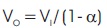
where, α is the triggering pulse cycle.
By varying triggering pulse cycle, the boost regulator output voltage changes and it is always higher than the input voltage which is provided by the solar PV system. The main benefit of boost regulator is to maintain solar input as well as output current continuously; the boost regulator can be implemented with MPPT system to maintain output voltage higher than the input voltage coming from solar PV system (Ho et al., 2012; Bruckner & Holmes, 2005).
The given topology is utilized for single-phase reduced device count five level inverter for photovoltaic applications. The proposed scheme reduces triggering stress across devices, improves harmonic profile and is capable of generating high power from the same available dc input power.
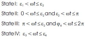
The proposed scheme as mentioned in Figure 3 is a combination of a single-phase two-level H-bridge conventional converter with a two bi-directional gate switch connected as an anti parallel combination. (Rai, Chaturvedi, Shimi, & Dwivedi, 2016).The input DC power is taken from a solar PV array and divided into equal parts by using two capacitors of same parameter and by using appropriate control technique, five different voltage levels (2V, V, 0, -V, -2V) can be achieved across the load. The two bi-directional gate switches Q1 and Q2 control the flow of current which flow through a common point of the two separate DC voltage sources. The voltage rating across switches Q3, Q4, Q5, and Q6 is identical to the DC bus voltage, i.e. 2V and similarly voltage across switches Q1 as well as Q2 is identical to V which is equal to half the total DC bus voltage. Therefore, cost of two switches Q1 and Q2 may be less than other switches. The anti-parallel combination of diodes provides continuous flow of current to maintain a constant sinusoidal output current. The operation of this inverter is divided in four triggering states as shown in Figure 4. State I has the voltage level of 2V (from 0.5 to 1), State II has the control range V (from 0 to 0.5), State III has the range of –V (from 0 to -0.5) and State IV has the range of -2V (from -0.5 to -1).
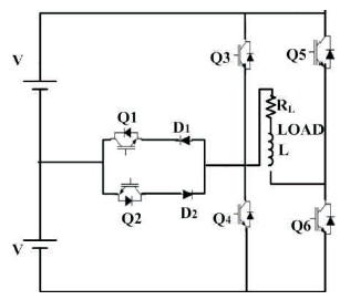
Figure 3. Reduced Device Count 5-Level Inverter
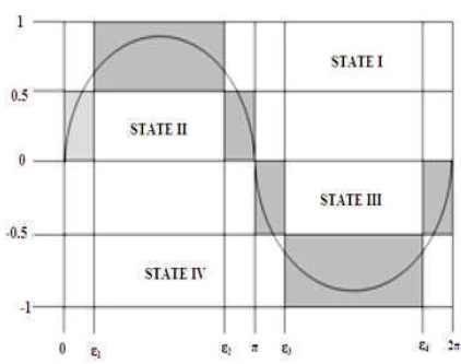
Figure 4. Triggering States of Multilevel Inverter
The different Triggering states of 5-level inverter are given in Table 2. The Zero voltage level can be achieved by having two different Triggering combinations.
The control principle of triggering signal for each device is mentioned in Figure 5 wherein the phase opposition carrier disposition PWM (POCDPWM) technique is implemented. Here, for generation of one complete cycle of fundamental frequency of 50 Hz, the inverter operates in four triggering states. (Gupta, Ranjan, Bhatnagar, Sahu, & Jain, 2015). Every set state has an upper level as well as lower level of voltage, as illustrated in Table 1. The different levels of output voltage are obtained by different gate triggering arrangement as illustrated in Tables 1 and 2. The upper voltage level “0*” and a lower voltage level “0” have the same value but it can be achieved with two different gate triggering state combination. However, to achieve the zero voltage level, different gate triggering configuration is required which can be achieved by different commutation schemes, as in the first half cycle, the output voltage is not same as that in the next half cycle, as seen from Figure 4. The time interval of each state varies according to the amplitude for the required output sinusoidal voltage (Banaei & Salary, 2012). The phase angles of different state changes from ε1, ε2, ε3 and ε4 and determine the time that the inverter operates within a certain state. The four states fall within the following boundaries:
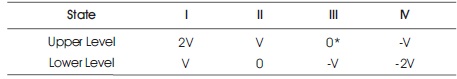
Table 1. The State Operation of Proposed Multilevel Inverter
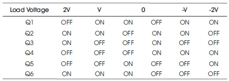
Table 2. Gate Triggering States Combination for Multilevel Inverter
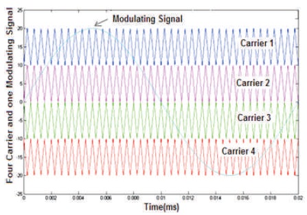
Figure 5. Generation of Control Signals for Each Device
Phase opposition carrier disposition PWM (POCDPWM) technique is implemented to regulate and arrange the reduced device count 5-level inverter. Here, to correlate n- multi level inverter system to provide a section voltage waveform with n-1 levels and the zero, n-1 multi carrier signals are needed (Nagarajan, Immanuel, & Boobalan, 2016). They all have a similar peak-peak amplitude as well as frequency, and every structure is specified in such a way that all carriers are contiguous.
The amplitude modulation index, Mai governs the different phase angles. The amplitude modulation index for the 5-level inverter with a phase opposition carrier disposition PWM (POCDPWM) is defined as:

Where, Ac is peak to peak value of per unit (pu) carrier signal (triangular in nature) and Am is per unit peak value of the modulating signal (sinusoidal in nature). Additionally, the frequency of Ma is defined as:

Here, fc is the carrier signal frequency (triangular in nature) and fo the modulating frequency signal (sinusoidal in nature).
If Am ≥ Ac consistently, i.e. the amplitude modulation index is greater than 0.5, the exchanging phase angles are defined as:


If Am ≤ Ac consistently, i.e. the amplitude modulation index m c is lower than 0.5, the exchanging phase angles are equal to:

Hence, from the above it is clear that the inverter neither operates in State I nor in State IV, if the modulation index is less than 0.5 and it generates only a three state of output voltage. Therefore, during the first half cycle, when Ma > 0.5, the inverter output voltage has three state specifically (0, V & 2V) and similarly during the next half cycle the inverter output voltage has another three states specifically (0, -V & -2V) as mentioned in Table 2. Switch Q5 turn OFF for first half cycle and turn ON for the next half cycle in opposition, on the other hand switch Q6 turn ON for the first half cycle and turn OFF for the next half cycle. Since Q5 and Q6 triggering frequency are equal and opposite for the 50 Hz fundamental output frequency, therefore power device such as BJT which is a low frequency device can be used in place of IGBTs. From Table 2, it is also observed that triggering of Q1 is also opposite to Q3, similarly triggering of Q2 is also opposite to Q4 it means that if Q1 switch is ON, Q3 switch will be OFF and similarly when Q2 switch is ON, Q4 switch will be OFF and vice versa.
The frequency of carrier signal (fc) and modulating signal is 2 kHz and 50Hz, respectively. The decision signals of PWM are calculated by comparing carrier signals with modulating signal, as shown in Figure 5. Here, Carrier 1 is represented by C1 with intersections of modulating signal; Carrier 2 is represented by C2 with intersections of modulating signal; Carrier is represented by C3 with intersections of modulating signal; Carrier 4 is represented by C4 with intersections of modulating signal. One cycle of output is a combination of six regions and these regions are defined in Figure 6. The different phase angle states of this region are given by ε1, ε2, ε3 and ε4 as shown in Figure 6. These six regions are defined below:
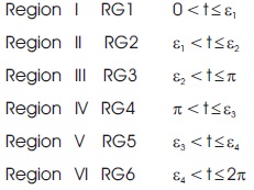
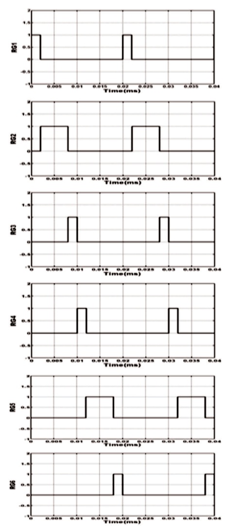
Figure 6. Output Regions of Gating Signals
The PWM decision signals have been obtained from the output region pulses, as mentioned in Figure 7 (Chaudhary, Parmar, & Sikander, 2019). The building of the switch triggering pulses from the triggering states of Table 1, the generated gating signals are shown in Figure 8. Now, it is feasible for each switch to describe the triggering signal. By using the logical gate, the Boolean terminology would be implemented and the triggering functions are given by:
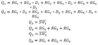
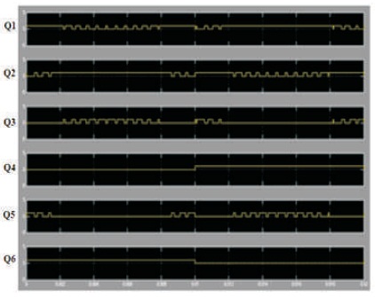
Figure 7. Control Triggering Signals of Inverter Switches
Figure 8. Decision Signals Generated
For below than 0.5 amplitude modulation index, the duration of the regions RG2 and RG5 may be zero. Though, the above logic still produces the appropriate switch triggering signals to generate the required output. Since the amplitude modulation index is below than 0.5, the multilevel inverter output reduces to three levels as stated earlier.
Multilevel inverter are used to convert DC voltage into five level or three level AC signal by changing the modulation index (Ma) from 1.0 to 0.4. When the Ma is more than or equal to 0.5, then five-level operation is achieved and when the Ma is lower than 0.5, then multilevel inverter operation goes into three-level State.
All the simulation results are obtained before filter and after filter with input DC voltage 140V and load is RL type where R=50 ohm and L=200mH . It is seen that by varying Ma, the output voltage of five-level inverter also varies. For Ma=1, the waveforms of voltage and current as mentioned in Figures 9-10 and before filter the voltage Vrms = 71.88V and current Irms= 4.329 A and voltage THD=28.43% is mentioned in Figure 11 and current THD = 1.51% as mentioned in Figure 12. Correspondingly, the waveforms of voltage and current after filter are shown in Figures 13-14 and after filter voltage Vrms =188.1V and current Irms = 2.342 A and the voltage THD=0.45%, as mentioned in Figure15 and current THD=0.45%, as shown in Figure 16.
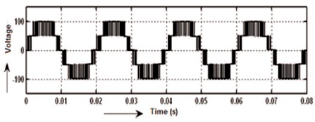
Figure 9. Before Filter 5-level Output Voltage Waveform of Inverter
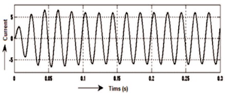
Figure 10. Before Filter 5-level Output Current Waveform of Inverter
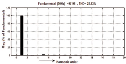
Figure 11. Before Filter 5-level Output Voltage Harmonic Spectrum of Inverter
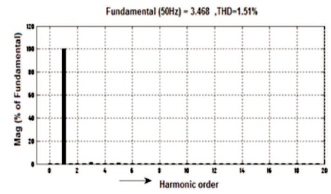
Figure 12. Before Filter 5-level Output Current Harmonic Spectrum of Inverter
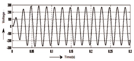
Figure 13. After Filter 5-level Output Voltage Waveform of Inverter
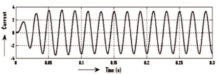
Figure 14. After Filter 5-level Output Current Waveform of Inverter
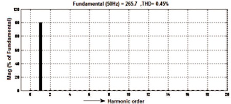
Figure 15. After Filter 5-level Output Voltage Harmonic Spectrum of inverter
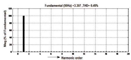
Figure 16. After Filter 5-level Output Current Harmonic Spectrum of Inverter
The waveforms of voltage and current before filter are shown in Figures 17-18, Vrms = 41.76 V and current is Irms = 2.455 A and the voltage THD = 36.77%, as shown in Figure 19 and current THD = 1.51%, as mentioned in Figure 20. Similarly, the waveforms of voltage and current after filter are shown in Figures 21 and 22, Vrms =106.7V and current is Irms = 1.328 A. and the voltage's THD = 0.45%, as shown in Figure 23 and Current's THD = 0.45%, as shown in Figure 24.
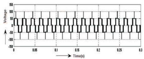
Figure 17. Before Filter 5-level Output Voltage Waveform of Inverter
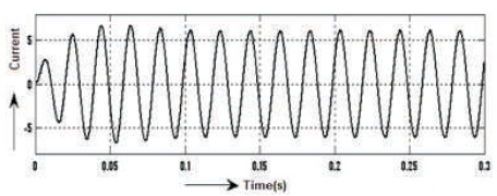
Figure 18. Before Filter 5-level Output Current Waveform of Inverter
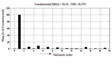
Figure 19. Before Filter 5-level Output Voltage Harmonic Spectrum of Inverter
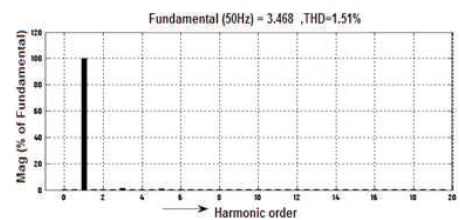
Figure 20. Before Filter 5-level Output Current Harmonic Spectrum of Inverter
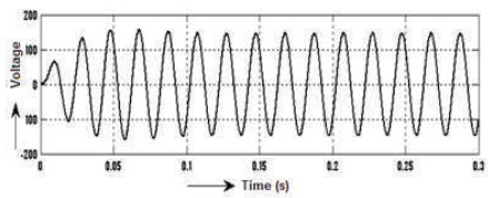
Figure 21. After Filter 5-level Output Voltage Waveform of Inverter
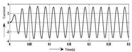
Figure 22. After Filter 5-level Output Current Waveform of Inverter
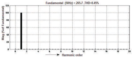
Figure 23. After Filter 5-level Output Voltage Harmonic Spectrum of inverter
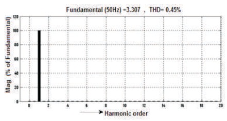
Figure 24. After Filter 5-level Output Current Harmonic Spectrum of Inverter
The waveforms of voltage and current before filter are shown in Figures 25-26, voltage is Vrms=40.74V, current Irms= 2.395A and voltage THD=36.92%, as shown in Figure 27 and Current's THD=1.53%, as can be seen in Figure 28. Similarly, voltage and current waveforms after Filter are shown in Figure 29-30, voltage is Vrms=104V and current Irms= 1.296 A and voltage THD=0.51% and Current's THD=0.46%, as shown in Figures 31 & 32.
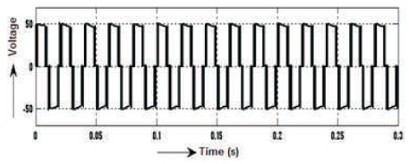
Figure 25. Before Filter 3-level Output Voltage Waveform of Inverter
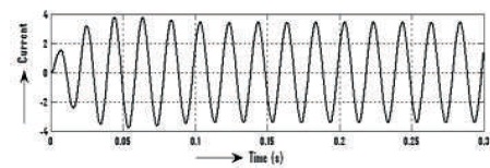
Figure 26. Before Filter 3-level Output Current Waveform of Inverter
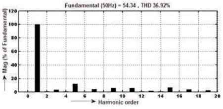
Figure 27. Before Filter 3-level Output Voltage Harmonic Spectrum of Inverter
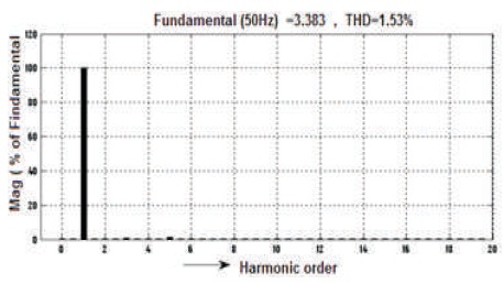
Figure 28. Before Filter 5-level Output Current Harmonic Spectrum of Inverter
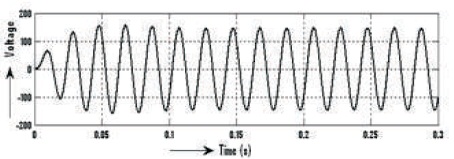
Figure 29. After Filter 3-level Output Voltage Waveform of Inverter
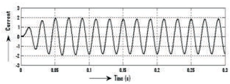
Figure 30. After Filter 3-level Output Current Waveform of Inverter
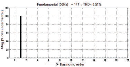
Figure 31. After Filter 3-level Output Voltage Harmonic Spectrum of Inverter
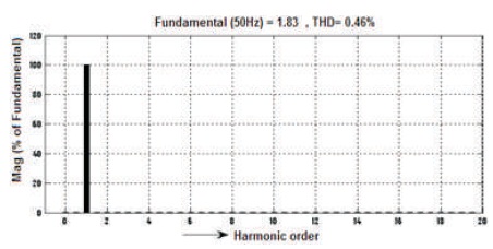
Figure 32. After Filter 3-level Output Current Harmonic Spectrum of Inverter
The summery in Table 3 shows that after filter the output voltage is increased where as current decreases during change in Ma =1, 0.5 and 0.4, where as the total harmonic distortion of multilevel inverter after filter in terms of voltage and current decrease for Ma=1, 0.5 and 0.4, as shown in Table 4.
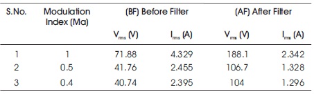
Table 3. Output Voltage and Current after Filter with Change in Modulation Index (Ma)
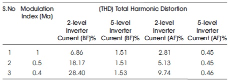
Table 4. Total THD in Terms of Current before and after Filter with Change in Modulation Index (Ma) for 2-level and 5-level
As per above analysis, it is clear that for Ma=1, the 2-level inverter has a very high value of THD, it is about 6.86% when triggering is done for fundamental output current. But it may have low cost and weight as compared to other topologies. In terms of weight calculations for 2-level inverter, filter cost and weight should be considered because in practical output current with 6.86% THD is not acceptable, whereas the cost and the weight of the 5- level multilevel inverters seem better when Ma = 1, measured before filter, current THD is 1.51% and after filter current THD is 0.45%. Similarly for Ma = 0.5 and 0.4, measured THD current, before filter and after filter is shown in Table 4. After filter Vrms voltage increases but current decreases, as shown in Table 3. The cost and weight of the multilevel inverter will be increased if the number of levels increases. In this work, 5-level phase opposition carrier disposition PWM (POCDPWM) topology is implemented along with the appropriate logic circuit to drive the multilevel inverter switch gating triggering signals with solar PV array system. The 5-level inverter output waveforms are produced if modulation indexes are more than 0.5 and if the modulation indexes are below 0.5, then 3-level output waveforms are produced.