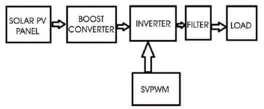
Figure 1. Layout of Solar Power Generation System
ln this paper, performance of solar photovoltaic power system using State Vector Pulse Width Modulation technique is studied. As we know the solar photovoltaic power generation is getting a wide attention because of its clean and renewable energy, which is the need of the hour to use as an alternate to the conventional energy. However, the power produced by solar PV system contains some power quality problems such as low output voltage, harmonics, ripples, and poor power factor. SVPWM techniques can be applied to reduce such problems. Such methods will be studied in this paper of solar PV power generation containing boost converter.
As we know, the increasing concern to find and use the alternate of the conventional energy generation is essential, the energy produced by fossil fuel is not only limited, but also affects the environment and contributes in a very large scale to the problem of global warming. A wide research and application of clean energy for power generation such as solar power, wind power, and hydro power is going on with a good pace.
Since the availability of sun is everywhere, solar power generation can be at any place both at large scale and small scale. Large scale power generation can be used to supply power to a big population or can be connected with the grid of conventional power system. Small scale solar power generation can be used for different applications such as for operation of motor, domestic loads, water pump, etc.
Solar power generation also has some issues such as high initial cost, unreliable in cloudy season, output power from inverter is not purely sinusoidal, output power contains harmonics, power factor, etc.
Solar power system includes power electronics converters such as DC-DC converter, Inverter, etc. Filters can be used for reduction of ripples in the output power waveform.
Gate signal can be provided with Sinusoidal Pulse width Modulation (SPWM) or Space Vector Pulse Width Modulation (SVPWM) and can be applied for power factor correction and for reducing harmonics. Boost converter used in the system increases the efficiency and SVPWM technique reduces the harmonics and corrects the power factor of the system. Overall working of solar power system with methods to improve its performance is studied in this proposed system.
The proposed solar power system mainly consists of five components. These components are;
Design of photovoltaic solar power system is very simple. The photovoltaic array is used to produce the DC output power from the solar radiations. The DC output of the solar panel is not good enough and it needs some boosting. A boost DC–DC converter is used for this purpose. As the name suggest the boost converter increases the overall power of the DC output produced by solar panel. This DC power is converted to AC by using an inverter. The gate signaling of the thyristors used in inverter is provided with a Space Vector Pulse Width Modulation. This particular technique for gate signaling is used to control the harmonics at the output of the inverter and improving the power factor. A filter is also used at the output of the inverter to get a ripple free waveform. The layout design is given in Figure 1.
Figure 1. Layout of Solar Power Generation System
Solar photovoltaic panel is made up of photovoltaic cells. These photovoltaic cells are made up of semiconductor that converts the solar radiations into electrical energy. These photovoltaic cells are made when n type material is in metallurgical contact with the p type material. In such way, a PN junction is formed. At the junction, electrons from n region diffuse into p region and combine with holes and produce negative charge. The opposite action also takes place producing a positive charge. The net result of it results in disappearance of conduction electrons and holes from the vicinity, stablishing a reverse electric field forming a depletion area. When light falls on front surface of photovoltaic and when photon energy exceeds the energy gap, it moves to the conduction band generating electron hole pair and thus producing electrical output [1].
A solar PV cell is shown in Figure 2. The source current Ip is photovoltaic current, D is diode, Rth and Rs is shunt and series resistance respectively[2].
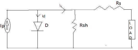
Figure 2 Solar PV Cell
The mathematical representation of solar cell is,
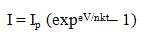

Voltage across diode will be
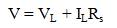
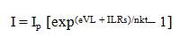
Where VL is the load voltage,
IL is load current,
T is the module operating temperature,
K is Boltzmann's constant,
Id is diode current.
It is a DC –DC converter that increases the DC voltage level at the output. As the name suggest, it boosts the input DC voltage and improves the voltage level. For this reason it is also known as the step up dc transformer. As shown in Figure 3, it contains one switch which is typically MOSFET or IGBT, one diode, one capacitor, and one inductor. The output DC power of the solar panel is given to this boost converter. The inductor used at the source is the prime factor behind the boost of voltage as it resists the change in current[3].
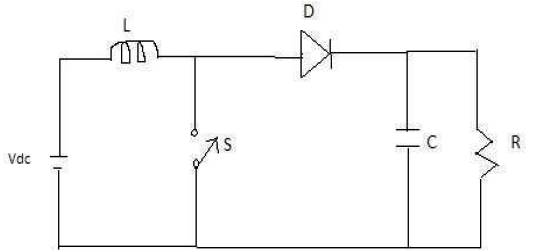
Figure 3. Boost Converter
It operates in two cycles. During the OFF state when the switch is closed, the current flows through inductor and stores some energy. In ON state when switch is opened, the inductor current passes through diode and capacitor and the stored energy in inductor is transferred at output and therefore the output voltage level is increased or get boost.
The mathematical representation of boost converter is,
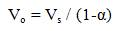
Where Vo is the output voltage,
Vs is the source voltage,
α is the duty cycle,
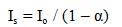
Is is source current,
Io is output current.
An Inverter is a DC–AC converter widely used in power electronics. It converts the DC input into AC output. These converters are categorized into two categories; current source inverter and voltage source inverter. A three phase voltage source inverter is shown in Figure 4. It consist of six thyristors which are generally IGBT and six diodes connected in three legs of the inverter. These elements are connecting to a three phase load. The three phase voltage source inverter generates less harmonic distortion in the output voltage. Pulse modulation is used to provide gate signaling to the IGBTs. The output of the inverter is never purely sinusoidal. Pulse Width Modulation schemes helps in achieving it to a far extend. The Sinusoidal Pulse Width Modulation or the Space Vector Pulse Width Modulation is used to reduce the total harmonics in the system that are introduced due to the use to power electronics converters. For three-phase SPWM, three modulating signals that are 120 degrees out of phase with one another are used in order to produce out of phase load voltages[3].
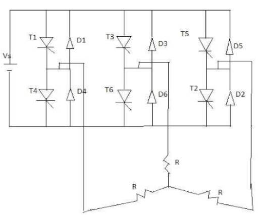
Figure 4. Three Phase Voltage Source Inverter
The mathematical output of inverter is,
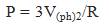
PWM inverter will inject ripple current in to the grid. The output LC filter is connected to remove high switching frequency components from output current of inverter. We should consider a low pass RLC filter at the output terminals of the inverter in order to reduce the switching frequency to a significant level. A typical low pass RLC filter is shown in Figure 5.
Figure 5. Low Pass Filter
It is a modulation technique which is used to control the voltage of the inverter internally. It is used as a control technique by applying controlled gate triggering to the switches used in the inverter [4]. It has few advantages such as;
In a three phase voltage source inverter, many PWM techniques are being used namely single PWM technique, multiple PWM technique, Sinusoidal Pulse Width Modulation (SPWM), and Space Vector Pulse Width Modulation (SVPWM).
In SPWM technique, the high frequency triangular carrier signal and sinusoidal reference signal are generated. The PWM signal thus generated is then used as triggering pulses to operate the switches. SPWM increases the order of dominant harmonics so that they can be filtered easily.
The other control technique is SVPWM. This control scheme can be used to overcome the shortcomings of SPWM. SVPWM can be realized more easily digitally and output voltage is higher for the same DC link voltage and the harmonics and switching losses are low. SVPWM control has a wide range of application from all kinds of AC drives to all kinds of power production system.
Space Vector Pulse Width Modulation (SVM) for three-leg VSI is based on the demonstration of the three phase quantities as vectors in a two-dimensional plane. Three phase inverter has eight switch status and are arranged accordingly in the sequence of a, b, c. Assuming that a switch is considered as 1 when it is switched on otherwise 0. Let us consider Wa , Wb and Wc as phase voltages and Wab, Wbc and Wca as line voltages. The transformation from three phase coordinates to two dimensional are shown in Table 1 which shows the relationship between switch state and voltages [5].
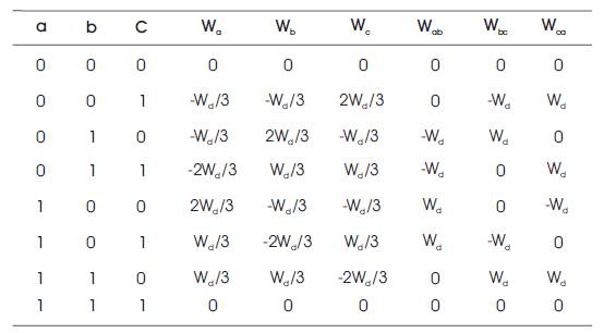
Table 1. Relation between Switch side and Voltage
Through three phase to two dimension converter, we can get eight combinations of phase voltages. Out of these eight voltages, six are non-zero voltage (V1-V6) and two are zero voltage vectors (V0, V7). These six non-zero voltage forms the six axis of the hexagon and separated by each other at an angle of sixty degrees [7]. The other two zero voltages are located at the coordinate origin.
Figure 6 shows space vector voltage in two dimensional plane.
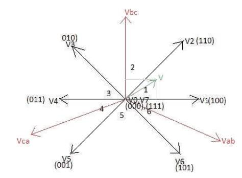
Figure 6. Two Dimension Space Voltage Vector
The preferred three phase voltages at the output of the inverter could be symbolized by an equivalent vector V revolving in the counter clockwise direction. The size of this vector is related to the magnitude of the output voltage and the time of this vector taken to complete one revolution is the same as the fundamental time period of the output voltage[6].
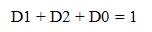
Let us consider the situation when the desired line-to-line output voltage vector V is in sector 1 as shown in Figure 7. This vector could be synthesized by the pulse-width modulation of the two adjacent space voltage vectors V1 and V2 the duty cycle of each being D1 and D2, respectively, and the zero vector (V7/V8) of duty cycle D0.
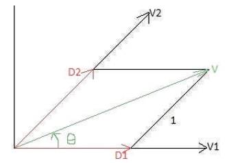
Figure 7. Required Output Voltage at Sector 1
Mathematically,
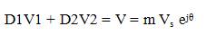
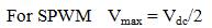
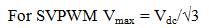
Where Vdc is DC link voltage and m is modulation index.
This means that Space Vector PWM can produce about 15 percent higher than Sinusoidal PWM in output voltage[8].
Hence any desired output voltage can be synthesized by Pulse Width Modulation of two adjacent voltage vector in any required sector[9].
MATLAB software contains Simulink model that provides a large number of standard modules to achieve a variety of basic functions and different modules. Such Simulink model of PV power generation, boost converter fed sinusoidal PWM controlled inverter and boost converter fed SVPWM controlled inverter are shown below.
Figure 8 shows the Simulink model of PV array that produce power of 100 KW. This PV array has 88 parallel strings and 7 series connected modules per string. The irradiance is 2 used as 1000 w/m with threshold temperature of 45 degree Celsius.
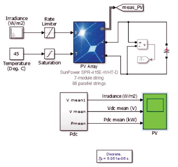
Figure 8. Simulink of PV Array
Figure 9 shows the Simulink diagram of the boost converter fed sinusoidal PWM controlled inverter and similarly Figure 10 shows the Simulink diagram of the boost converter fed sinusoidal PWM controlled inverter.
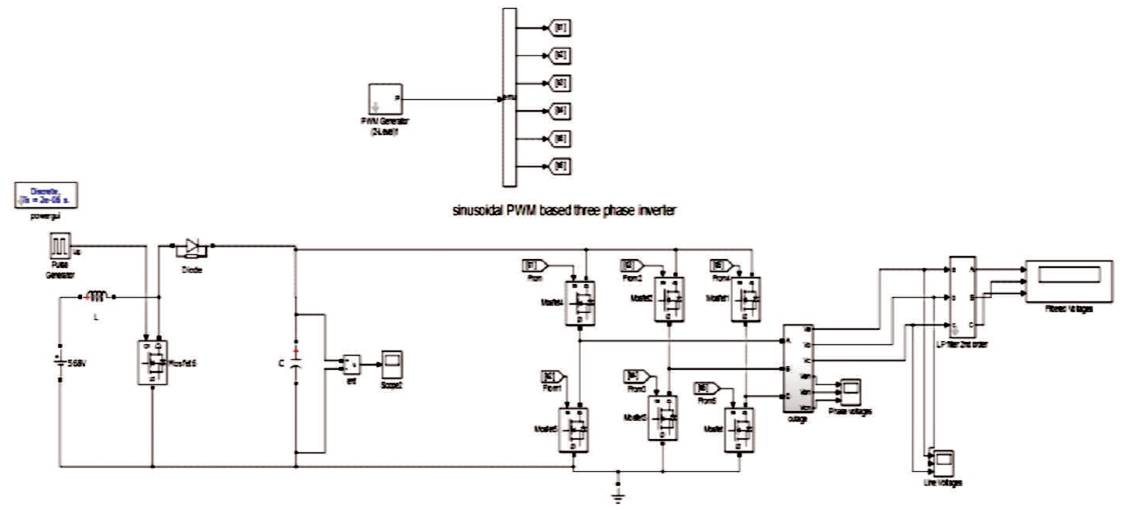
Figure 9. Simulink of Sinusoidal PWM Controlled Inverter
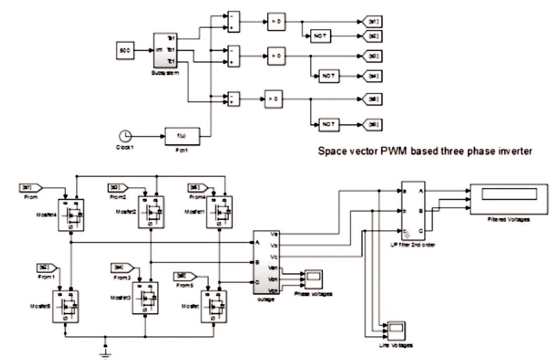
Figure 10. Simulink of SVPWM Controlled Inverter
Figure 11 shows the relevant simulation waveforms of the PV module. Figure 11(a) shows the photovoltaic array output voltage, while Figure 11(b) shows the photovoltaic array output power[10]. The output voltage is calculated to be 568 V and the output power is calculated to be about 100 KW.
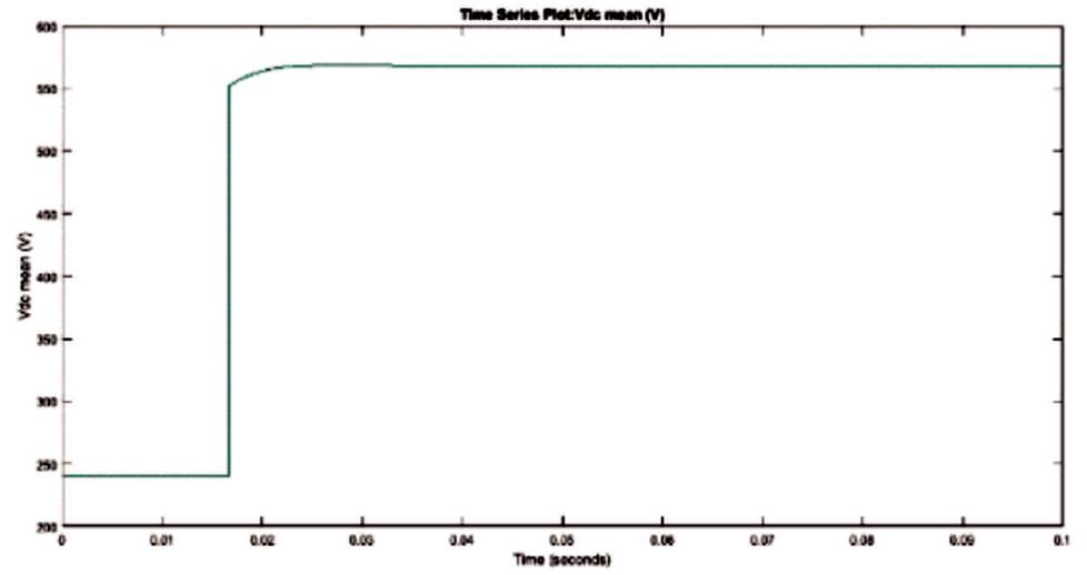
Figure 11(a) PV Output Voltage Mean (Vmean)
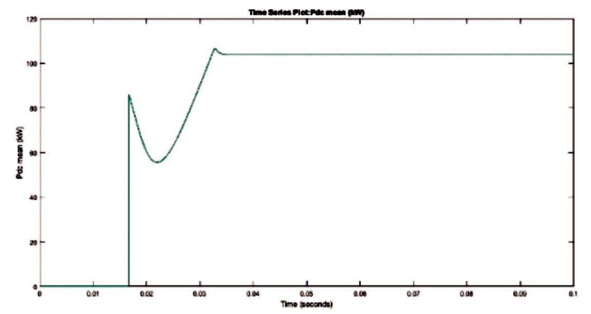
Figure 11(b) PV Output Voltage Mean (PMean)
Figure 12 shows the relevant simulation waveforms of sinusoidal PWM controlled inverter, and the filtered output voltage of phase A. Its output voltage is calculated to be 1500 V. The output waveform is clearly visible to have many distortions and harmonics.
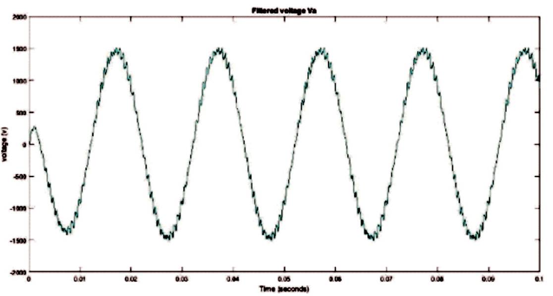
Figure 12. Output Voltage of Sinusoidal PWM Controlled Inverter
Similarly, Figure 13 shows the relevant simulation waveforms of SVPWM controlled inverter, and the filtered output voltage of phase A. Its output voltage is calculated to be 1680 V. The output waveform is clearly visible to have very low distortion and harmonics.
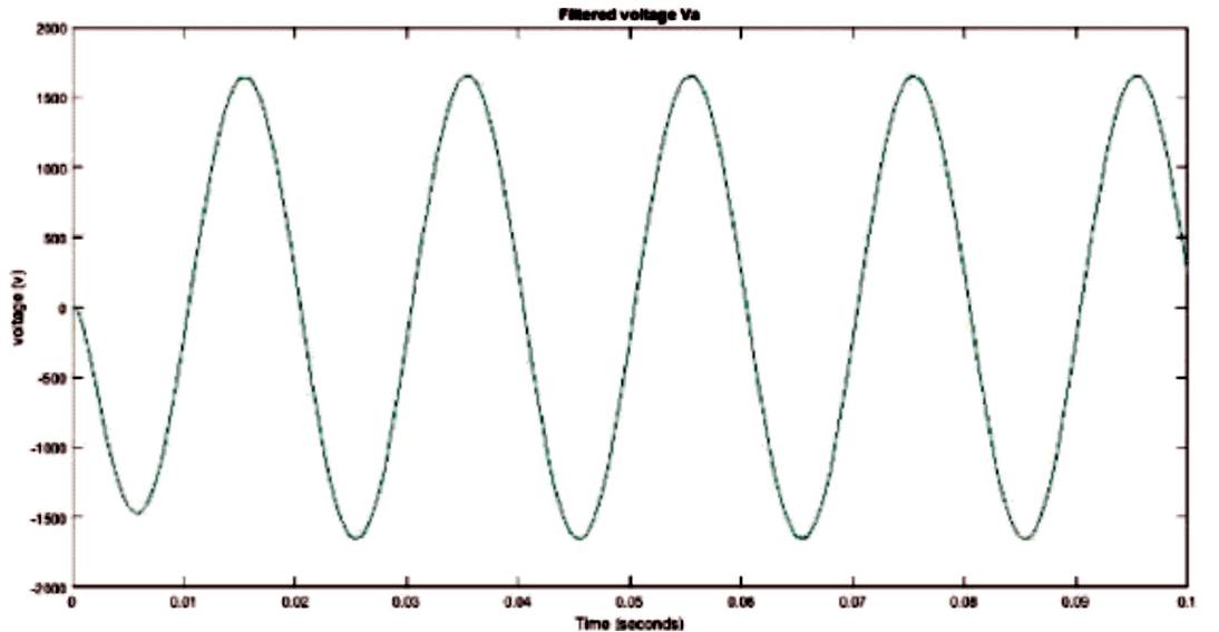
Figure 13. Output Voltage of SVPWM Controlled Inverter
The electricity sector in India is still banking on conventional energy resource for power production. The solar power production can solve many issues related to conventional power systems such as deficit of fuel, shortage of clean and authentic energy resources, insufficient coal- fired, oil-fired and natural gas-fired thermal power plants reduction in global warming, etc. The wide research on performance enhancement of solar power has discovered some highly advanced control technologies that can replace the existing ones for better performance of the solar system. The control technique studied in this paper shows that the Space Vector Pulse Width Modulation technique provides higher output voltage and reduces harmonics to a significant level and is better than all the existing PWM schemes. However, SVPWM technique is very complicated and involves too many inverter switching states. So the use of this technique should depend on the application after analyzing its advantages and drawbacks