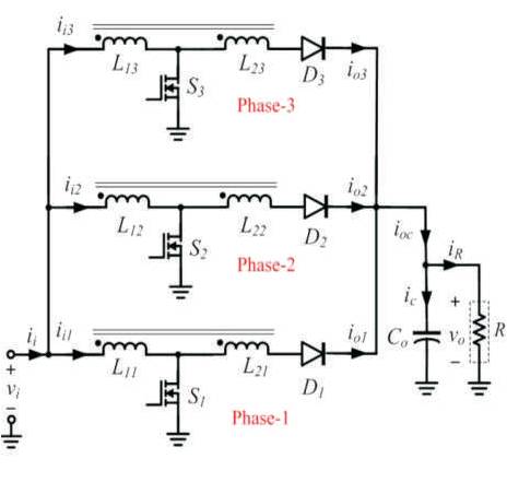
Figure 1. Three-phase interleaved converter with ideal coupled - inductor boost converters
This paper presents a Three-phase Non isolated Inter leaved Boost Converter (IBC) for high step up operation. Threephase IBC has a number of boost converters connected in parallel with same switching frequency. Three-phase IBC are highly preferred to reduce the ripple current. A boost converter is used to clamp the voltage stresses of all the switches in the Inter leaved converter which is caused by the leakage inductance. This paper focuses on the leakage energies of the interleaved converter and are collected in a clamp capacitor and then recycled to the separate load by the clamp boost converter. Simulation and experiment results have been performed to understand the efficiency of three-phase IBC and the results have been validated.
In Renewable energy applications, highefficiency, highvoltage step-up DC-DC converters are required as an interface between the available low voltage sources and the output loads, which are operated at much higher voltages[1]-[5]. In many industrial applications, it is required to convert a fixed DC voltage source into a variable voltage source. A DC converter can be considered as DC equivalent to an AC transformer with a continuously variable turn's ratio. Like a transformer, it can be used to step down or step up a DC voltage source. DC converters are widely used for traction motor control in electric automobiles, trolley cars, marine hosts, forklift trucks, and mine haulers. They provide smooth acceleration control, high efficiency, and fast dynamic response. DC converters can be used in regenerative braking of DC motors to return energy back into the supply, and this feature results in energy savings for transportation systems with frequent stops[6]-[12]. DC converters are used in DC voltage regulators in conjunction with an inductor, to generate a DC current source, especially for the current source inverters. The boost converter is widely used in single phase Power Factor Correction (PFC) converters because its input current is continuous and the topology is simple.
Renewable energy sources, such as photovoltic cell and fuel cells, have quite low voltage output and require series connection or a voltage booster to provide enough output voltage. High step up gain, high efficiency and non - isolation are the main characteristics for these applications [13]-[17]. Large input current and high - output voltage are the two major concerns for high step up converters. The high-step-up DC-DC converters can be Non isolated but they should operate at high efficiency while taking high currents from low voltage DC sources at their inputs.
In conventional boost converter, the duty ratio increases as the output to input voltage ratio increases. Therefore, the conventional boost converters will require extreme duty ratios to meet the high voltage step-up requirements [18]-[22]. In three-phase IBC the duty ratio selection is based on the number of phases, the ripple is minimum at a certain duty ratio.
In conventional boost converter the extreme duty-cycle operation drives short-pulsed currents with high amplitude to flow through the output diodes and the capacitors, which cause severe diode reverse recovery problem and increases in the conduction losses [23]-[27]. The reverse recovery problem will degrade the efficiency and limit the power level of conventional boost converter. To overcome these problems three phase interleaved boost converters has been proposed to interface with renewable energy source.
Three-phase IBC operates at a minimum duty ratio due to a high output voltage and a low input voltage. Interleaved method is used to improve converter performance in terms of efficiency, electromagnetic emission and transient response. To minimize the amount of ripples, Three-phase IBC has been proposed in addition to which it has improved performance characteristics of higher power capability, modularity and improved reliability [28]-[30]. However IBC improves converter performance at the cost of additional inductors, switching devices and output rectifiers.
Interleaved boost converters are mainly used for Renewable energy sources. Three phase Interleaved boost converters has a number of boost converters connected in parallel with same switching frequency is shown in Figure 1 Furthermore, all the phases are operated at the same duty ratio, but they are phase shifted by 2π/n radian electrical angle (n = 3). The input currents and output currents of these interleaved phases are shown in Figure 2. To lower the voltage stress on the switches, a common active-clamp circuit is connected to the boost converter is shown in Figure 3. The active clamp circuit in each phase, in which a clamp-diode (Dc1, Dc2, . . Dcn ) is connected to the common node of the primary inductor, the secondary inductor and the switch of an interleaved boost converter. The cathode terminals of all the clamp diodes are connected to a clamp capacitor Cc. The energies stored in the leakage inductors of the interleaved phases are discharged through the clamp diodes and gathered in the clamp capacitor Cc. Furthermore, the boost converter is used to transfer the stored energy in the clamp capacitor to the output of the interleaved converters.
Figure 1. Three-phase interleaved converter with ideal coupled - inductor boost converters
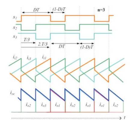
Figure 2. Gate pulses, primary inductor currents and output capacitor charging current of Three-phase Interleaved boost converter
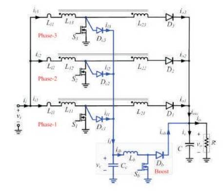
Figure 3. Three-phase interleaved boost converter with single active clamp
The energy stored in all the leakage inductances of the interleaved boost converter are discharged to the capacitor (Cc ).To clamp the switch voltages of the interleaved converter, the voltage of this capacitor has to be controlled. The boost converter transfers the leakage energy stored in the Clamp capacitor (Cc ) to the output and maintains its voltage to a desired clamp voltage level. So, the power rating of the clamp boost converter is decided by the maximum total leakage energy of the interleaved converters.
Therefore, the voltage at the output of the clamp boost converter is decided by the interleaved boost converters. The duty ratio of the clamp boost converter can be controlled to discharge the leakage energy stored in the Clamp capacitor (Cc ) to the output dc bus. In threephase IBC the ripple is minimum at a duty ratio in the range of 0.66.
The clamp boost converter can be operated either in Continuous Conduction Mode (CCM) or in Discontinuous Conduction Mode (DCM). Under CCM, the switching losses are more than the switching losses under DCM. However, the conduction losses under the DCM are more than the conduction losses under the CCM. MOSFET is used in clamp boost converter to maintain high voltage levels. Therefore, the clamp boost converter is chosen to operate in Discontinuous Conduction Mode (DCM) to reduce the losses.
The design aspects of 3-phase IBC are discussed in this section:
The Voltage gain of the converter can be obtained as
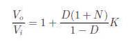
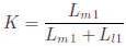
Where Vo is the output voltage, Vi is the input voltage, D is the duty ratio, N is the turns ratio, K=0.97, Lm1 is the magnetising inductor and Ll1 is the leakage inductor.
Reverse bias Voltage is maximum across the secondary side diode Do1 can be obtained as
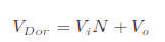
Where VDor is the Reverse bias Voltage.
Total Leakage power can be calculated from all leakage inductances
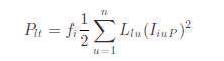
Where fi is the switching frequency of interleaved coupled inductor boost converter, Llu is the primary leakage inductance and Llu P is the peak primary inductor current in the uth phase.
The value of boost inductor can be found out by the following formulae
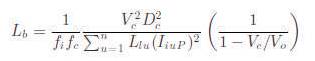
Where fc is the switching frequency of clamp boost converter, Dc is the Diode, Llu is the primary leakage inductance and Iiu P is the peak primary inductor current in the uth phase.
The simulation is done using Matlab simulink and results are presented. Scope is connected to display the output voltage. The converter consists of three interleaved coupled-inductor boost converters and a common clamp boost converter.
The interleaved converter is designed to operate at a switching frequency of 25 kHz. The calculated lower limit of the clamp voltage of the designed converter is about 120 V. To limit the fall time of the leakage inductor current is about 2 μs, the clamp voltage level of the converter is designed to be 140 V. This clamp voltage value decides the maximum voltage stress of the switches of the coupled-inductor boost converter. The measured input and output voltages of the converter are 42 and 350 V, respectively. Figure 4 shows the Simulated diagram of interleaved converter.
The high voltage spikes caused by the leakage inductors can be successfully reduced to a lower level by the proposed clamp boost converter. The output voltage level and the clamp voltage levels of the converter under full load condition are presented. The total input current of the converter is presented. The currents in the primary inductors of the three phases of the interleaved converter are also shown. The phase currents are equal in amplitude and phase shifted by 120◦. The leakage inductance is discharged to the clamp-capacitor in the form of a current spike. The input and output voltage waveform is shown in Figure 5.
The efficiency of the converter is 95.4%. The simulation results show that 3-phase IBC can successfully handle the high-input current and perform voltage step-up operation at a high efficiency.
The switching circuit is simulated and results are shown in Figure 6. Scope is connected to display the output voltage. Output waveforms across the switching circuit with and without leakage energy is shown in Figure 7 and 8.
Non Isolated Interleaved boost converter with a common active clamp is developed and tested in the laboratory.
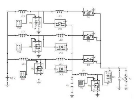
Figure 4. Simulated diagram of Interleaved Boost Converter
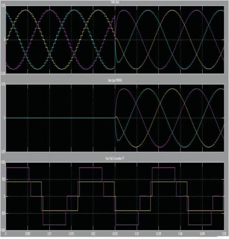
Figure 5. Input and Output Voltage waveform for Interleaved DC-DC Converter
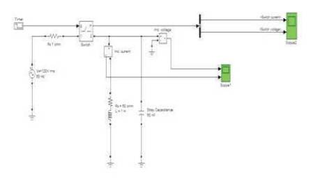
Figure 6. Simulated diagram of Switching circuit
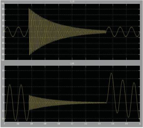
Figure 7. Switching losses with leakage inductance
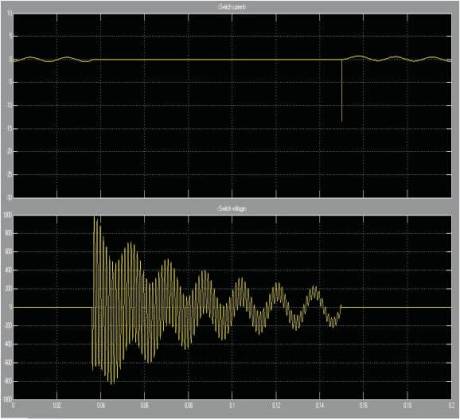
Figure 8. Switching losses without leakage inductance
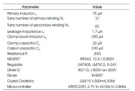
Table1. Optimum for design specifications
The following values are found to be a near optimum for the design specifications are shown in Table 1.
The coupled inductors of the interleaved converter are designed with KoolMμ KE5528 E-cores. The primary winding of the coupled inductor has 21 turns (125 × 40 litz wire, three parallel wires) and the secondary winding is made of 62 turns (125 × 40 litz wire, single wire). The switching frequency of the converter is 25 kHz. The measured input and output voltages of the converter are 42 and 350 V, respectively. The clamp voltage is maintained at 140 V.
The clamping arrangement is done to clamp the voltage across the switch to a low level, close to the voltage stress offered by an ideal coupled inductor. The slope of the leakage current is decided by the leakage inductor and the voltage difference between the clamp voltage and the voltage at the common node of the primary and secondary inductors. The fall time of the leakage current is close to 2μs. The measured leakage currents from all the three interleaved coupled-inductor boost converters shown in Figure 9, will charge the clamp capacitor.
Pulses required by the MOSFETs are generated by using a ATMEL microcontroller 89C2051. These pulses are amplified by using a driver amplifier shown in Figure 10. The gate pulses to the MOSFET of the clamp boost converter and the inductor current is presented. The output voltage of DC converter is shown in Figure 11,12,13.
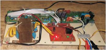
Figure 9. Experimental set - up Interleaved Boost converter
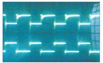
Figure 10. Driving pulses for Mosfets(X axis 1unit = 0.5μs,Y axis 1unit = 5V)
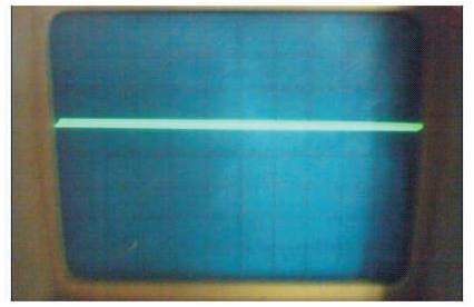
Figure 11. DC output voltage X axis 1unit = 1ms,Y axis 1unit = 10V
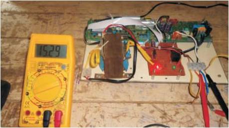
Figure 12. Output voltage with switching losses
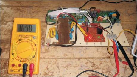
Figure 13. Output voltage without switching losses
This paper portrays a Three-phase non isolated interleaved boost converter for high step-up power conversion. In coupled inductor boost converter the switch is subjected to high voltage stress due to leakage current present in the non ideal coupled inductor.The various waveforms of IBC have been simulated using MATLAB Simulink. The proposed converter reduces the voltage stress of the switches. Interleaved boost converter uses clamp capacitor for collecting leakage energies from all coupled inductor boost converter. The converter achieves high efficiency because of the recycling of the leakage energies in reduction of the switch voltage stress. Non isolated interleaved boost converter is suitable for high current and high power application. The converter achieves high efficiency high reliability with reduced size inductors and capacitors. The Matlab Simulation results and Experimental results show that the converter reaches to high efficiency because of the recycling of the leakage energies. From the experimental results it proves that output voltage without switching losses is more.