(1)

This paper reported a rare earth Holmium (Ho) doped copper indium sulphide CuInS2 (CIS) thin film grown by using very economical chemical bath deposition method. Bath temperature was kept constant at 80oC. The main aim of this work is to synthesize a good photosensitive semiconducting film which can be used in photovoltaic devices like solar cells. The SEM images shows that the synthesized film is uniform, densely packed with cubic like grains. X-ray diffractogram confirms chalcopyrite and wurtzite phase of CuInS2. Absorption peaks are blue shifted which is due to decrease in particle size. EDAX shows that synthesized film is non-stoichiometric and confirms the doping of Ho. It is found that initially transmittance is low in UV region but increases in visible region. Higher transmittance of 90% is obtained between 540-620nm. Thus this film can be used in solar cells. Reflectance is low in the synthesized film showing that the film is anti reflection substance. The Ho doped film possesses larger band gap of 2.2 eV as compare to bulk film of CuInS2 which is due to reduced particle size. Refractive index and extinction coefficient calculated in this film are 1.79 and 0.03 respectively. Ho doped CuInS2 film is quite good photosensitive material. A strong emission peak is obtained at a wavelength of 630 nm in the IR region. The photoconductive gain calculated for the sample is ~2.6×10⁴,which is quite good.
The studied ternary compounds Cu-III-VI2 (III = Ga, In and VI = S, Se) are direct gap semiconductors with tetragonal chalcopyrite (CH) crystal structure. These materials are relevant in various fields, including nonlinear optics, optoelectronic, and photovoltaic devices (Ohmer, & Pandey, 1998; Birkmire, & Eser, 1997; Shirakata, Chichibu, Isomura, & Nakanishi, 1997). Accurate knowledge of the optical functions of these materials is very important for many of these applications. Copper indium sulphide (CuInS2) is an important ternary compound which has been investigated for its plentiful applications. CuInS is a direct band gap material with a phase transition temperature of 980°C. CuInS2 has various advantages with a narrow band gap of 1.53 eV (Yao et al., 2014) making it insensitive to temperature with good stability. It has high absorption coefficients, mostly at 105 cm-1, and can absorb 90% of sunlight for films of 1 to 2 μ m thickness. All these advantages make CuInS2 one of the most promising alternative absorbing semiconductor materials for the development of thin film solar cells (Yao et al., 2014; Li, Li, Zhao, Shi, & Teng, 2014). CuInS2 has anti- interference properties, a strong ability to resist radiation, a long service life, and lower toxic species compared to CuInSe2. Among different chalcopyrite semiconductors it has much potential as a thin film solar cell. The theoretical efficiency obtained for a CuInS2 thin film solar cell is between 28 and 32% (Siemer, Klaer, Luck, & Bräunig, 2001) but the highest conversion efficiency observed is only 13% (Binsma, Giling, & Bloem, 1982; Goto, Hashimoto, & Ito, 2004), which is notably less than the predicted theoretical value. Various methods for the synthesis of CuInS2 thin film have been reported including reactive radio frequency magnetron sputtering (Liu & Shao, 2007), co-evaporation (Gossla, Metzner, & Mahnke, 2001), ion layer gas reaction (Qiu, Jin, Qian, Shi, & Wu 2005) spray pyrolysis (John et al., 2017) and chemical bath deposition (Pathan & Lokhande, 2004; Tiwari & Tiwari, 2006). The Chemical Bath Deposition (CBD) method is somewhat simple, inexpensive and highly reproducible technique. By CBD method, the dimensions of the crystallites can be assorted controlling deposition parameters like pH, reaction time, temperature and presence of impurities in the solution (Sankapal, Sartale, Lokhande, & Ennaoui, 2004). CBD is a method of growing thin film of certain materials on a substrate immersed in an aqueous bath containing appropriate reagents at temperatures ranging from room temperature to 100 oC. Therefore it is intended to synthesize films by CBD technique using appropriate impurities and complexing agents to control reaction rate and hence to investigate the corresponding changes in structural and optical properties.
Rare earth element Ho doped CuInS2 thin film grown from a solution of highly pure and analytical reagent grade of CuCl2.2H2 O(99%), In Cl3 (99%) and thiourea (99.8%) in an alkaline solution of ammonia and double distilled water. Microscopic glass slides used as substrates are cleaned many times in double distilled water, HCl and acetone ultrasonically. The glass slides are kept vertically in a solution bath. The deposition of CIS:Ho films are done by adding 10 ml solution of copper chloride {CuCl2.2H2O(0.1 M)}, 10 ml of Indium chloride {InCl3(0.1M)}, 2ml of triethylamine (TEA), 20 ml of thiourea (0.1M) in a beaker in which 10 ml of ammonia is added for the maintaining pH of the solution. Then 0.001 M of impurity is added with 6 ml concentration to the basic solution of CuInS2. Film deposition is the consequence of precipitation followed by condensation on glass substrates. Thin films are prepared at 80 oC bath temperature for 1 hour. The prepared films are homogeneous, well adhered to the glass substrate.
The X-ray diffraction patterns of the CIS films doped with Ho prepared on glass substrates is shown in Figure 1. It is found that the film consist of peaks corresponding to both chalcopyrite and wurtzite phase of CuInS2. Thus polytypsim structure is identified. No peaks corresponding to Ho is observed which shows that doping of rare earth element doesn't change the structure. The relationship between grain size and line broadening can be described by Scherrer's formula,
where λ represents the wavelength of X-ray light, β, and θ are the Full Width at Half Maximum (FWHM) of a peak, and the Bragg's angle respectively. The grain size 'D', the strain value 'ε' and the dislocation density 'δ' is calculated corresponding to the prominent peak (004) CH. These values are summarized in Table 1.
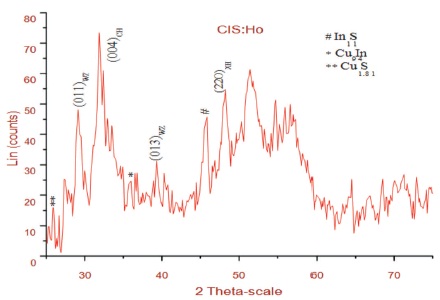
Figure 1. XRD of CIS:Ho Doped Thin Film
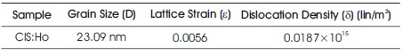
Table 1. Value of Grain Size, Lattice Strain and Dislocation Density
The surface morphology of CuInS2: Ho thin film is analyzed using Scanning Electron Microscopy (SEM) technique at 250 X, 500 X and 5000 X and shown in Figure 2. It is clear from the SEM images that the film is almost uniform, densely packed and smooth with only few very small pinholes or cracks and are composed of cube-like grains. The synthesized film is highly agglomerated.
Figure 2. SEM Images of CIS:Ho Doped Thin Film
The concentration of the films has been studied by EDAX analysis. The presence of Cu, In, and S and Ho concentrations has been identified and shown in the EDAX spectra of Figure 3. The presence of oxygen in the films may be incorporated either from the atmosphere or from the aqueous medium. The concentration of indium (In) is high in rare earth doped film. The film is nonstoichiometric. In Table 2 experimental values obtained from EDAX is shown.
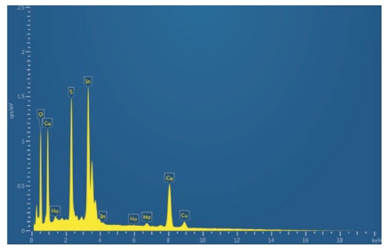
Figure 3. EDAX Images of CIS:Ho Doped Film
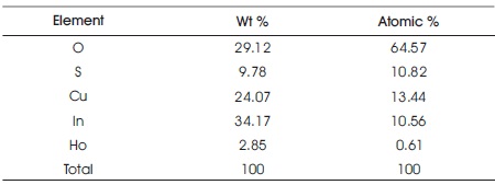
Table 2. Experimental Values of CIS: Ho Thin Film Obtained from EDAX
In Figure 4 transmittance spectra of Holmium (Ho) doped CuInS2 (CIS) film has been shown in the wavelength range 320-840 nm. The film is having 90% transmittance between 540-620 nm. Thus this material is having good scope to be used in solar cells. In Figure 5 reflectance of CuInS2: Ho film is shown. The value of reflectance is found to be very low in ultraviolet, visible and infrared area. As wavelength increases reflectance decreases but then there is a small increase in reflectance. Thus the synthesized film with rare earth element is anti reflection material. In Figure 6 absorption spectra is shown. The absorbance spectrum shows a steep increase in absorption at wavelength near to the absorption edge of the threshold wavelength for onset of absorption. It is clear that absorption edge is flat in Ho doped CIS film. It may be due to appearance of more energy levels corresponding to impurities in the band gap. The absorption peaks are blue shifted in Ho doped CIS films as compare to that of the bulk CIS (band gap = 1.53 eV, λmax= 810 nm). This blue shift in absorption is due to decrease in particle size in comparison to the bulk material. With decreasing size of the particle, binding energy of exciton increases because of the increasing columbic overlap enforced by spatial localization of the wave functions (Guha, Das, Maity, Ganguli, & Chaudhuri, 2003). The band gap energy (Eg) and absorption coefficient (α) of the synthesized CuInS2:Ho film is determined from the absorption data. The absorption coefficient (α) can be calculated by,

where c is a constant. The value of absorption coefficient obtained is 105 cm-1 in the visible region. The high value of absorption coefficient makes it valuable for the production of high absorptive layers of solar cell.
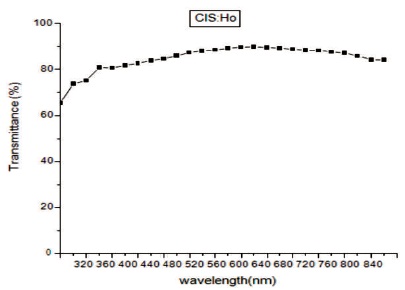
Figure 4. Transmittance Spectra of CIS:Ho Doped Film
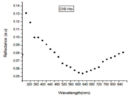
Figure 5. Reflectance Spectra of CIS:Ho Doped Film
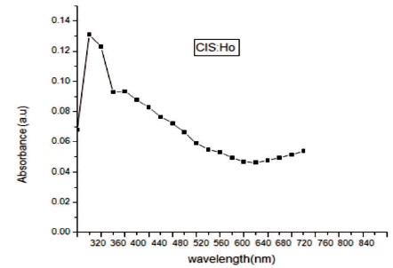
Figure 6. Absorbance Spectra of CIS:Ho Doped Film
In Figure 7 a graph is plotted between (αhν)2 and photon energy (hν). As CuInS2 is a direct band gap material the extrapolation will give the value of band gap. The band gap obtained for Ho doped film is 2.2 eV. The band gap of undoped CIS film obtained is 2.19 eV as discussed in earlier paper of the authors (Sengupta, Pateria, & Deshmukh, 2018). The larger band gap is due to decreasing particle size. The levels corresponding to valence band are shifted to lower energy side but levels of conduction band are shifted to higher energy side. Using the hyperbolic band model the authors studied the optical properties of synthesized CuInS2 thin film. Average particle size has been calculated by using equation (Sheikh, Khajuria, Sanotra, Khajuria, & Singh, 2016).
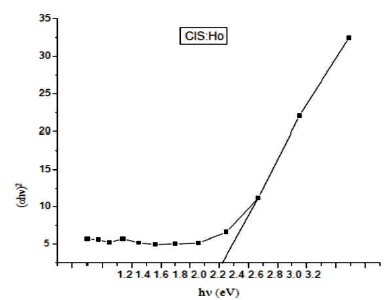
Figure 7. Graph Plotted between (hαν) and hν

where m* is the effective mass of the electron, Egn and Egb are the band gap of nano and bulk sample. The calculated value is 1.25 nm. The refractive index and extinction coefficient of the film has been calculated for l=820 nm by the formula (Kariper, 2014) and listed in Table 3.


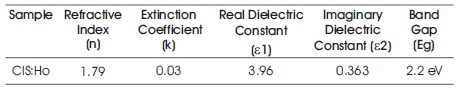
Table 3. The Value of Band Gap, Refractive Index (n), Extinction Coefficient (k), Real and Imaginary Dielectric Constants (ε1, ε2) for CuInS2 :Ho Thin Film at λ=820 nm
In Figure 8 photoluminescence emission spectra of undoped and CIS:Ho doped thin film are recorded between 300-1000 nm by exciting it at wavelength 450 nm. Photoluminescence is a process in which a molecule absorbs a photon in the visible region, exciting one of its electrons to a higher electronic excited state, and then radiates a photon as the electron returns to a lower energy state. A strong emission peak is obtained at a wavelength of 630 nm in the IR region corresponding to 2.2 eV in both undoped and doped film. The red band is due to the transition of electron from deep level to valence band (Abken, Halliday, & Durose, 2009). The only difference is the intensity. The intensity of CIS:Ho doped film is high. This may be due to the greater thickness and improved crystallinity of films.
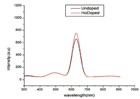
Figure 8. Emission Spectra of CIS:Ho Film
In Figure 9, rise and decay curve of CIS:Ho is shown. For this study a 100 W incandescent lamp is used. Photo current flows due to photo carriers when light falls on it. It is clear that at first photo current increases and then it gets saturated. The decay of the current is slow. The photoconductive gain calculated for the sample is ~2.6×10⁴, which is good. In Figure 10, a graph is plotted between dark current (Id.c) and voltage. Electrodes are made of silver. Voltmeter and ammeter are used for measuring voltage and current by connecting in series. It is found that according to Ohm's law as voltage increases, current also increases linearly. From the dark current study, we can conclude that the conductivity of the synthesized film is good.
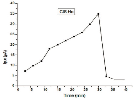
Figure 9. Rise and Decay Curve of CIS:Ho Film
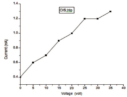
Figure 10. Graph between Id.c and voltage
The film of CuInS2 with rare earth element holmium (Ho) has been synthesized successfully by chemical bath deposition method on the microscopic glass slides. The synthesized film is having polytypsim structure with multiphase. The SEM images shows that the synthesized film is uniform, densely packed with cube like grains. Agglomeration of particles can be viewed clearly in SEM images. In EDAX, intense peak of Cu, In, S along with Ho confirms the doping of Ho. The presence of oxygen was observed which may be added from the atmosphere. The film is non-stichiometric. The transmittance of the deposited film is high ~90% between 540-620 nm. Thus this material is having good scope to be used in solar cells. The value of reflectance is found to be very low in ultraviolet, visible and infrared area. Thus the synthesized film with rare earth element is anti reflection material. The absorbance spectrum shows a steep increase in absorption at wavelength near to the absorption edge of the threshold wavelength for onset of absorption. Absorption edge is flat in Ho doped CIS film. It may be due to appearance of more energy levels corresponding to impurities in the band gap. The absorption peaks are blue shifted. This blue shift in absorption is due to decrease in particle size in comparison to the bulk material. The band gap of the film obtained is 2.2 eV. A strong emission peak is obtained at a wavelength of 630 nm in the IR region. The photoconductive gain calculated for the sample is ~2.6×10⁴, which is quite good.
Author are very much grateful to the management of CSIT, Durg and SSGI, Bhilai for their constant support to pursue the research work. Also, the authors are thankful to SAIF, Cochin for XRD, SEM and EDAX studies.