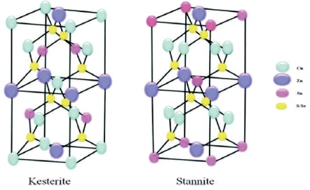
Figure 1. Kesterite and Stannite Structure of CZTSe (Zopi, 2009)
In the second generation thin film solar cell, Copper Zinc Tin Selenium (CZTSe) thin film is considered as the quintessential absorber layer in solar cell as its constituents are earth abundant and non-toxic, making it environmental friendly. Many fabrication methods have been employed to fabricate the films like Thermal evaporation method, pulsed layer deposition, RF-DC Sputtering, etc. The authors have monitored the aspects that highly influence the band gap of CZTSe thin films during the deposition process. This paper recapitulate the parameters that affect the band gap of CZTSe thin film as an absorber layer like substrate temperature, annealing temperature, and order of precursors.
As the population is ever increasing and main energy production is by fossil fuels, which affects the environment directly, it is time to look forward to use renewable energy resources more than to utilize this abundant energy source. Among all the available renewable energy resources, solar energy is considered as the most important consistent and abundant source of energy. Copper Zinc Tin Selenium (CZTSe) has emerged as a deserved candidate for thin film solar cell with the band gap lying in the visible region of electromagnetic spectrum. CZTSe is a quaternary semiconductor and exhibits the following properties:
CZTSe compound is reported to exist in two structures, namely Kesterite and stannite type. Both of these structures are identical except that the positioning of copper and zinc atoms is different. It is difficult to assign the crystal structure based on X-ray diffraction techniques alone: the difference in the scattering cross-sections between Cu and Zn is small, and hence similar diffraction patterns are produced for kesterite, stannite, and all related partially disordered phases, While the vibrational spectra of the two materials are also similar, the change in lattice symmetry results in an appreciable difference in Raman intensities (Hong et al., 2012). An arrangement of its constituent's atoms, which makes the difference between the Kesterite and stannite structure is shown in Figure 1.
Figure 1. Kesterite and Stannite Structure of CZTSe (Zopi, 2009)
CZTSe has been emerged as a p-type absorber layer for thin film solar cell because of its high absorption coefficient and its suitable band gap of 1.5 eV lying within the visible region of the electromagnetic spectrum. In a CZTSe hetero-junction, second generation thin film solar cell Molybdenum (Mo) is taken as a back contact, where Resistive Zinc Oxide (ZnO) layer is placed between the conducting layer and the window layer to obstruct shunting. CZTSe has attracted attention exponentially due to less expensive and earth abundant material (Lai, Yang, Wei, & Kuo, 2017).
Photovoltaic technology has attained an admirable growth during the last decade due to global energy scenario as tremendous accretion in population is causing an excruciating increment in electricity demand. Switching over to renewable energy technology offers a number of benefits with providing a good contribution to the energy supply. The present invention in thin film solar cells is going on to find out the best substitute material and to increase the efficiency. The Copper Zinc Tin Selenium (CZTSe) thin films have been emerged as an absorber layer in thin film solar cell. Many vacuum and non-vacuum thin film deposition techniques like thermal evaporation, RF-DC sputtering, Pulsed layer deposition, etc., are available to fabricate the CZTSe thin films. Its band gap is the important tool that characterizes the performance of CZTSe thin film solar cell so mainly the parameters like substrate temperature, annealing temperature, ratio, and order of precursors maintained during the deposition process highly affects the performance of reactively deposited CZTSe thin films are elaborated below :
To improve the stability and grow single phase structure, a single target was prepared by Wibowo, Kim, Lee, Munir, & Kim (2007) maintaining the stoichiometry of CZTSe structure to fabricate thin films implementing the RF-DC sputtering method. They reported the stannite phase containing Cu2Se concluding that the film prepared at 15 oC of substrate temperature exhibited an optical band gap of 1.56 eV. These results were based on the absorption spectra which presented value of absorption coefficient near 104 cm-1. These values presented good perspectives for photovoltaic applications. Babu, Kumar, Bhaskar, & Raja (2008) embodied the dependence of substrate temperature (in the range of 523–673 oK) on band gap of CZTSe thin films prepared by the thermal evaporation method and annealed at 723 oK. It was revealed by X-Ray Diffraction (XRD) patterns that at the substrate temperature of 523 oK and 573 oK secondary phases of Cu2-xSe was detected, while at Ts= 673 oK secondary phase of ZnSe along with Cu2ZnSnSe4 was observed. A slight increment in the band gap of thin films with annealing was also observed.
Polycrystalline CZTSe thin films were fabricated exerting RF-DC magnetron sputtering method with substrate temperature of 200 oC. The hall measurements sanctioned the formation of p-type absorber layer with an optical band gap of 0.9 eV and crystallized in stannite phase with lattice constants a= 5.684 Å and c= 11.353 Å (Zoppi et al., 2009).
Luckert et al. (2011) molded Cu2ZnSnSe4 thin films on molybdenum coated glass substrates by the magnetron sputtering and selenisation process concluding that the occurrence of an excitonic peak was the reason of high quality films with uniform deposition with band gap of 1.01 eV at room temperature. Cu2ZnSnSe4 thin films were formulated by consecrating the thermal co-evaporation method by Park et al. with the results that deposited CZTSe exhibited two main Raman peaks at 170 and 192 cm-1 possessing band gap of 0.99 eV at room temperature (Park et al. 2011). Han, Chen, Wan, & Xu (2012) framed CZTSe thin films by the using two step method manipulating Co-electroplating of Cu, Zn, and Sn followed by selenisation process maintaining the different substrate temperature. This was concluded that the substrate temperature strongly controls the phase formation in thin film during formation process as increasing substrate temperature removed the secondary phases of CuSe and SnSe.
Brammertz et al. (2013) deposited CZTSe thin film as an absorber layer following two steps, including sputtered deposition of Cu, Zn, and Sn and post selenizaton of CZT precursor culminating the effect of potential barrier on the performance of CZTSe thin film solar cell as potential of 135 MeV of solar cell remained relatively small at room temperature, but there was an exponential increase of the series resistance at low temperatures. Kuo and Hsu (2014) sputtered Cu, Zn, and Sn precursors on Mo coated SLG substrate with TiN coating as reaction barrier layer and selenized the as deposited precursors for 1h in Se vapor. It was consummated that TiN coating improved its efficiency upto 3.7% with electrical conductivity of 2.9 Ω-1 cm-1 as it was 0.58% for TiN coating free substrate.
To study the characteristics of CZTSe thin films, Liu and Hu (2014) adopted single step electro deposition method. They fabricated it on Mo coated substrate with different deposition potential and deduced that Cu/Zn ratio decreased in the composition of CZTSe with increment in electrochemical deposition voltage, while band gap increased with this sequence and higher direct band gap was exhibited by the lower Cu/(Zn+Sn) ratio in composition as shown in Table 1.
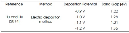
Table 1. Effect of Deposition Potential on Band Gap with Mo Coated SLG Substrate
Salome, Fernandes, & Cunha (2010) deposited single phase crystalline CZTSe thin films (selenisation of DC magnetron sputtered metallic precursors) in order to attain the band gap within the range of visible spectra. They reported that increasing the pressure during the growth of CZTSe thin film can reduce the loss of Sn due to the evaporation of SnSe. The solid state reaction method was adopted by Ahn et al. (2010) to fabricate CZTSe thin films concluding that below 300 oC no binary compounds were detected as its crystallization started above 300 oC. Above 300 oC all elemental powders mixed together to form Cu ZnSnSe . Further, it was derived that Se loss could 2 4 not be refrained during the reaction.
Exerting RF magnetron sputtering method, Kim and Amal (2011) prepared CZTSe thin films by post selenisation process of sputtered Cu-Zn-Sn alloy. It was eventuated that increasing the annealing temperature upto 500 oC improved grain size and crystal quality exhibiting p-type semiconductor nature with mobilities of 1.30 cm2v-1s-1 to 2 9.27 cm2v-1s-1. Shao, Zhang, Zou, & Xie, (2012) notify that CZTSe thin films obtained from the selenization process in argon atmosphere at 450 °C for 1.5 h processed by the thermal evaporation method exhibited the band gap of 1.52 eV and absorption coefficient of 104 cm-1.
Klavina et al. (2010) prepared CZTSe thin films laboring thermal co-evaporation of the elemental precursors on 1mm thick Mo coated soda lime glass. To inspect the electrical performance of CZTSe thin films with respect to the annealing temperature, annealing process was done at temperatures such as 320 oC and 370 oC. It was concluded that increment in the annealing temperature caused to further increment in the band gap from 1.0 eV to 1.21 eV.
Further, Cu-Zn-Sn precursors were sequentially sputtered on Mo coated Soda lime glass substrate following the selenisation process by Hong et al. (2012) with the inference that band gap of 1.17 eV was measured independent of annealing temperature ranging from 350 °C to 650 °C in steps of 50 °C with lattice parameters as a = 5.709 Å and c = 11.351 Å. Table 2 illustrates the variation in band gap with respect to annealing temperature recruiting thermal evaporation method.
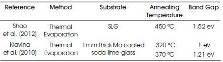
Table 2. Effect of Annealing Temperature on CZTSe Thin Films
Raman scattering measurements validated the presence of secondary phases of ZnSe accumulating towards the absorber surface with the excess of Zn completing the statement that increasing the annealing temperature lead to the diffusion of ZnSe to the back absorber region more strongly (Fairbrother et al., 2014). Absorption measurements have been used to supervise the changes in band gap energy (Eg) of CZTSe thin film as a function of the annealing temperature. It was concluded that deposition of precursor in ordered way caused to increment in E by the 110 meV in comparison to fully disordered material. Simulations in kinematics showed that Eg plays an important role as ordering parameter and the critical temperature for the CZTSe order-disorder transition is 200 ± 20 oC (Rey et al., 2014).
Redinger et al. (2014) deposited Cu2ZnSnSe4 (CZTSe) thin films using thermal co-evaporation method accompanied by high temperature annealing. To reduce the Sn loss, SnSe2 layer was evaporated on the absorber CZTSe layer resulting in the reduction of decomposition of CZTSe thin film. A solar cell with efficiency of 5.1% was designed.
Lai et al. (2017) have revealed that films prepared at the temperature below 500 oC employing thermal evaporation method on Mo coated SLG substrate showed Kesterite phase as increasing the temperature above 500 oC originated many voids at the bottom of the absorber layer deviating from the Kesterite phase due to Sn loss from elemental composition as confirmed by the SEM and EDX. Having a deep insight into the films of CZTSe prepared in the temperature range of 480-540 oC, it was concluded that band gap decreased from 0.93 eV to 0.88 eV increasing the temperature.
Babu, Kumar, Bhaskar, & Vanjari, (2010) have fabricated CZTSe thin films comprising Cu/(Zn+Sn) ratio in the range of 0.85 to 1.15 using four source co-evaporation method. Annealing process was done in selenium atmosphere for 1 hour. They concluded that thin films having Cu/(Zn+Sn) ratio of 0.90-1.10 exhibited single phase and polycrystalline structure while thin films of Cu/(Zn+Sn) ratio of 0.85 contained ZnSe as secondary phase. Juškenås et al. (2012) treated two step electrochemical mechanism to fabricate CZTSe thin films by the post annealing of CZT+Se in Ar atmosphere upto 500 °C. The XRD results of CZT precursor indicated the presence of ηCu6.26Sn5, Sn and γ-CuZn5 phases while CZTSe exhibited kesterite phase resulting towards more pure form of CZTSe with the fast increase in the annealing temperature. The effect of incorporation of Sodium on the performance of CZTSe thin film was consigned by Li, Kuciauskas, Young, & Repins, (2013) confirming that the incorporation of sodium increased the hole density resulting the shifting of Fermi level to lower level with higher open circuit voltage with higher fill factor and decrement in the width of depletion layer. With the statement that selenization time of deposited precursors strongly affects the growth of CZTSe thin films. He et al. (2014) processed CZTSe using the stacked elemental layer deposition technique with rapid thermal processing. The energy dispersive X-ray measurement confirmed the minor deviations of metal compositional ratio amidst the final thin films and the precursor as well as the crystallinity of CZTSe thin films were improved with the increment of selenization time.
Li et al. (2016) inspected the growth of CZTSe thin film prepared by using sputtering method optimizing the Se ratio. Effect of low Cu content was also sermonized as low Cu content showed higher open circuit voltage. 10.4% efficient solar cell without antireflection coating was constructed with Cu/(Zn+Sn)= 0.75. Kim, Park, Ryu, Oh, & Shin, (2017) have presented a work on the betterment of open circuit voltage of CZTSe thin film solar cell by inserting dielectric layer between CZTSe and surrounding layers. Inter diffusion of Cu and Cd was abrupted by inserting ~100 nm dielectric layer between CZTSe/CdS interface improving the fill factor and open circuit voltage. Yeranyan sedimented CZTSe thin films to scrutinize the effect of order of precursors on optical properties of CZTSe thin film on Mo coated SLG manoeuvring RF-DC sputtering method and sealed the work with conclusion that roughness was found bigger for precursor order Mo/Zn/Cu/Sn/Se rather than Mo/Cu/Zn/Sn/Se and reached to the result that thin film solar cell with better efficiency Mo/Zn/Cu/Sn precursor’s order should be preferred (Yeranyan, 2017) as mentioned in Table 3.

Table 3. Effect of Order of Precursor on Band Gap
A capacious range of deposition techniques has been explored for fabrication of CZTSe thin films as the novel progress in Cu2ZnSnSe4 has opened a new path of developing high efficient PV devices with low cost and low non-toxic materials. From the device point of view, it is highly warranted to have a look at its electric properties so the authors have summarized the current state of art of band gap for CZTSe deposited by using various method. The formation of secondary phase in thin films also affects the performance of thin films from the solar cell point of view. Review presented in this paper can be summarized as that excerption of befitting parameters concerning the deposition can highly enhance the electrical and optical properties suitable for photovoltaic application.