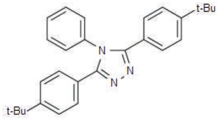
Figure 1. Structural Diagram of 3,5-Bis(4-tert-butylphenyl)- 4-phenyl-4H-1,2,4-triazole
This paper presents the surface morphological, optical and charge transport characterization of thermally evaporated thin film of organic material, namely 3, 5-Bis (4-tert-butylphenyl)-4-phenyl-4H-1, 2, 4-triazole (abbreviated as BBPT) prepared by well-known thermal evaporation technique, to be applied as an electron transport material in optoelectronic devices. Carrier mobility and AC conductivity are estimated from frequency dependent admittance characterization performed over a single layer device having structure ITO/ BBPT /Al and are found in the range 5.17 x 10⁻⁵ cm2 V-1s-1 and 4.83575 × 10⁻⁶ ohm-1 m-1, respectively. Various electrical parameters are calculated from charge transport characterization of ITO/ BBPT /Al device. Results of this work demonstrated that the conduction mechanism is in good correlation with the theory of hopping conduction in amorphous materials and the material studied have a potential application as an Electron Transport Layer (ETL) material in optoelectronic devices.
Optoelectronic devices like Photovoltaic Cells, Photodiodes, Light emitting diodes, etc., are among the most studied and promising devices in material science (Antohe, 2000; Reinhard et al., 2011; Kwon & Park, 2011; Friend et al., 1999; Tang, 1982). Among these, optoelectronic devices fabricated using organic materials with multilayered structure have revolutionized the research in this field due to low cost and considerable performance (Petritsch, 2000; Lee et al., 2011). The initial single layered structure was composed of emissive/absorbing layer sandwiched between a transparent anode (mostly indium doped oxide (ITO) coated glass) and a metallic cathode. However, the performance of optoelectronic devices like Organic Photovoltaic Cells (OPVCs) and Organic Light Emitting Diodes (OLEDs) based on this single layered configuration was not considerable due to blockage of charge carriers at electrode/semiconductor contact (Petritsch, 2000; Mitschke & Bauerle, 2000 ). From the last few decades, different approaches have been applied to reduce the carrier blockage at electrode/semiconductor interface to boost the performance of these devices. Among all, the incorporation of an electron-transport layer (ETL) between the emissive layer/absorbing Layer and cathode is a highly efficient and effective approach to improve the performance of optoelectronic devices (Friend et al., 1999; Lee et al., 2011; Mitschke & Bauerle, 2000; Rees et al., 2002; Strohriegl & Grazulevicius, 2002). In most of the organic semiconducting materials, electron mobility is lower than hole mobility (Kulkarni et al., 2004; Zhang & Jenekhe, 2000). So the proper material choice and their design is a crucial factor to fabricate highly efficient optoelectronic devices. One of the important roles of electron transport materials is to transport the electrons injected from cathode for efficient recombination with holes which results into emission of electrons. To be effective to boost the performance of OLEDs and OPVCs, an ETL material must possess: high electron mobility, high electron affinity to speed up the electron-injection, suitable HOMO and LUMO levels for efficient electron injection and hole blocking, high band gap with no absorption and emission in visible region, high glass transition temperature with thermal and chemical stability for uniform and crack free growth of thin films by thermal evaporation or spin coating, reversible electrochemical reduction, high triplet energy for exciton blocking, amorphous morphology in thin film configuration to prevent light scattering (Kulkarni et al., 2004; Zhang & Jenekhe, 2000; Antoniadis et al., 1994; Lee et al. 2014; He et al., 2004).
To date, only few ETL materials satisfy the above mentioned conditions to fabricate highly efficient OLEDs and OPVCs. Among them 1,2,4-Trizole derivatives with electron deficient triazole moieties (TAZ) shows high electron transporting and hole blocking behavior (Hung et al., 2005; Zhuang et al., 2012; Hsu et al., 2009; Kido et al., 1993). There are a number of reports on the role of 1,2,4-Triazole derivatives as electron transport materials to fabricate highly efficient OLEDs. Blue and green emission OLEDs with the use of 3,4,5-triphenyl-4H-1,2,4-triazole as an electron transport material shows excellent results due to its high thermal stability, bipolar properties, and good morphology (Zhuang et al., 2012). Bipolar host materials synthesized by the linkage of phenylcarbazole and 3,5-bis (2-pyridyl)-1H- 1,2,4-triazole are proved to be exceptional ETL materials to fabricate blue, green, yellow, and red OLEDs with significant efficiencies of 8.8%, 16.7%, 17.5%, and 16.7%, respectively (Hung et al., 2012). Meta coupling between 9H-carbazol-9-yl-phenyl and 3,4,5-triphenyl-4H-1,2,4- triazole results into highly efficient green and blue emission devices (Zhuang et al., 2012). Further, a large number of electron transporting materials like 3-(biphenyl-4-yl)-5-(4- tert-butylphenyl)-4-phenyl-4H-1,2,4-triazole (Hsu et al., 2009), 3-phenyl-4-(1′-naphthyl)-5-phenyl-1,2,4- triazole (Adachi et al., 2000), 3,5-biphenyl-4-phenyl(or 4-naphthyl)- 1,2,4-triazole (Tao et al., 2010), 3-(Biphenyl-4-yl)-5-(4-tertbutylphenyl)- 4-phenyl-4H-1,2,4-triazole (Tsai et al., 2006), etc. based on 1,2,4-Triazole moieties are reported to show excellent results in OLEDs.
Still, it is a necessity to investigate new electron transport materials to further improve the performance of optoelectronic devices. 3,5-Bis (4-tert-butylphenyl)-4- phenyl-4H-1,2,4-triazole (C28H31N3) shown in Figure 1 is a similar kind of material based on highly electron transporting 1,2,4-Triazole moiety.
Figure 1. Structural Diagram of 3,5-Bis(4-tert-butylphenyl)- 4-phenyl-4H-1,2,4-triazole
To study its applicability as ETL material, it is required to study its structural, optical, and electrical properties in this film configuration. Herein, thin film of 3,5-Bis (4-tert-butylphenyl)- 4-phenyl-4H-1,2,4-triazole is prepared on chemically and ultrasonically cleaned patterned ITO coated glass substrates by thermal evaporation. Structural and optical properties are studied for its possible use as an electron transport material. An ITO/ BBPT /Al device is fabricated and studied for Capacitance-frequency (C-f) characteristics to find various electrical parameters. Conduction mechanism is discussed by studying the variation of AC conductivity with frequency of signal applied to the device.
The material under investigation, 3,5-Bis(4-tert-butylphenyl)- 4-phenyl-4H-1,2,4-triazole was purchased in pure form, from Sigma Aldrich (India). Thin films of BBPT were prepared on chemically and ultrasonically cleaned quartz substrate by thermal evaporation using the Hind High Vacuum 12A4D vacuum coating unit. Evaporation of the materials is -5 done at base pressure of 10 Torr using a tungsten boat by keeping the evaporation rate constant at 7 Å/s. Thickness of films (~150 nm) was monitored by quartz crystal based thickness monitor assembled with vacuum coating unit. Surface Morphology of the film was studied using Field Emission Scanning Electron Microscopy (FE-SEM, Zeiss Supra 55). The surface topography and surface roughness of the film was analyzed by scanning an area of 10 x 10 μm using Atomic Force Microscopy (AFM) (Nanosurf easyscan2, Switzerland) in tapping mode. Grazing incidence X-ray diffraction (GIXRD) studies were carried out using Bruker D-8 system, which consists of a goniometer and a Cu K X-ray source (0.15405 nm). The angular step size for XRD studies was kept at 0.02o . UV–visible and fluorescence spectrum of film was studied using Shimadzu Spectrophotometer UV 2450 and Perkin Elmer LS-55 Spectrophotometer.
ITO/BBPT/Al device was fabricated by thermal deposition of BBPT on ultrasonically cleaned ITO coated glass substrates followed by deposition of Al electrodes using Hind High Vacuum 12A4D vacuum coating unit. Silver paste was used to make contacts of copper wires with Al and ITO electrodes. This device is then characterized for Admittance Spectroscopy using HIOKI 3522 and 3532 LCR high tester.
FESEM image of thermally evaporated BBPT thin film is shown in Figure 2(a). The smooth surface without any texture indicates the amorphous nature of film. The film is very uniformly deposited as only very few particulates are visible on the surface.
The surface morphology is further studied using Atomic Force Microscopy. Figure 2(b) shows AFM image of BBPT thin film. This image indicates an uniform and crack-free growth of film with observed Root Mean Squared (RMS) surface roughness of 12 nm. Small size grains having average base width of 140 nm are observed forming randomly distributed chains with length 2-3 μm. These chains of grains will improve the conductivity of BBPT film.
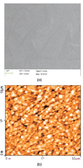
Figure 2. (a) FESEM and (b) AFM Image of BBPT film Prepared by Thermal Evaporation
To confirm the structural nature of BBPT film, grazing incidence X-Ray diffraction (GIXRD) is studied. Figure 3 shows the GIXRD pattern of BBPT film. No diffraction peak is observed in the XRD pattern, which declines any possibility shows the GIXRD pattern of BBPT film. No diffraction peak is observed in the XRD pattern, which declines any possibility of crystalline phase, confirms the amorphous nature of BBPT film.
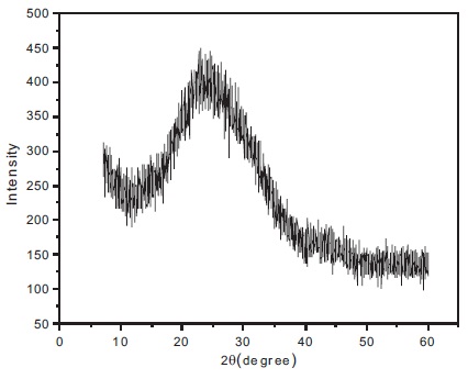
Figure 3. GIXRD Pattern of BBPT Film
Figure 4 shows the optical properties of BBPT film. UV-Vis absorption and emission spectrum of BBPT thin film is studied at room temperature in the wavelength range 200- 600 nm. Strong absorption peak is observed in the UV region from 290 to 330 nm with maximum absorption at 297 nm. It corresponds to the n–p* transitions of the 1,2,4- triazole groups. Strong optical emission peak is observed at 361 nm in the UV region when excited at 300 nm (inset Figure 4). Optical absorption and emission properties of BBPT film show that it is transparent for visible light, which is the basic necessity for a material to be used as a carrier transport layer in OLEDs and OPVCs. As a proof of the concept, an ITO/BBPT/Al device is fabricated. Figure 5 displays the variation of capacitance of ITO/BBPT/Al device with frequency at different operating voltages. It is observed that capacitance is strongly frequency dependent. At a fixed DC bias, capacitance decreases with increasing frequency and reaches a steady value of 0.626 nF.
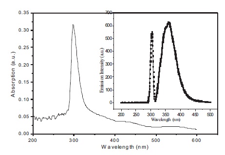
Figure 4. UV-Vis Absorption Spectrum of BBPT film Prepared by Thermal Evaporation (inset) Emission Spectrum of BBPT Film
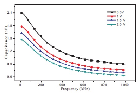
Figure 5. Variation of Capacitance of ITO/BBPT/Al Device with Frequency of AC Signal Applied
This obtained steady value of capacitance is the lowest value obtained at maximum frequency and maximum applied bias. So it should be equivalent to the geometric capacitance of the device given by Murtaza et al. (2011).
It is simply the capacitance of a parallel plate capacitor. Here, ɛo is the permittivity of free space, ɛ is the dielectric constant of BBPT, A is the area of the device = 3 mm2 , and d is the thickness of the deposited thin film = 150 nm. Using this relation for Cgeo , the value of electrical permittivity for BBPT is found to be equal to 3.14 × 10⁻¹¹C2N-1m-2 and 3.53, respectively.
In lower frequency range, increase of capacitance with the decrease in frequency is due to the blockage of charge carriers at the terminals. In dielectrics, a few charges exist, which can move for some distance through the dielectrics due to applied electric field. At the point when such charge carriers are hindered in their movement, they got trapped either in the material or on interfaces, since they cannot be freely discharged or replaced at the electrodes. The space charge layer so formed due to trapping of charge carriers in the material or at the electrodes results into an increase in the capacitance. However, as the frequency increases, the charges can easily move through the system, which therefore decreases the capacitance of the film. The observed decrease of capacitance with increasing frequency can likewise be explained on the basis of enhancing inability of the dipoles to orient them in a quickly shifting applied electric field. It is seen that the capacitance decreases in the lower frequency range with increase in frequency and attains a constant value at higher frequencies, which is an obvious trend in the dielectrics (Birey, 1978; Ridge et al., 1968).
Carrier mobility of BBPT film is calculated from the plot of differential susceptance [ω(C-CGeo)] (Jonscher, 1983; Vincent et al., 1975) versus frequency (ω). Figure 6 shows the variation of differential susceptance of ITO/BBPT/Al device with frequency (ω) at different biasing voltages. It is seen that differential susceptance increases with increase in frequency, reaches a maximum value at relaxation frequency (fr = 1/τr ) and then starts decreasing with increase in frequency (where τr is the relaxation time).
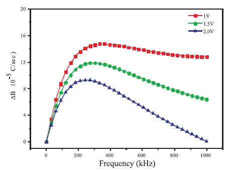
Figure 6. Variation of Differential Susceptance of ITO/BBPT/Al Device with Frequency of AC Signal Applied
Relaxation time is related to average transit time (tdc) by the relation tdc= 0.56 Tr. The hole mobility (μdc) is calculated using the following relation (Murtaza et al., 2011; Tsang et al., 2006).
where, 'd' and 'V' are the film thickness and bias voltage, respectively. The calculated values of relaxation time and hole mobility for BBPT film are listed in Table 1.
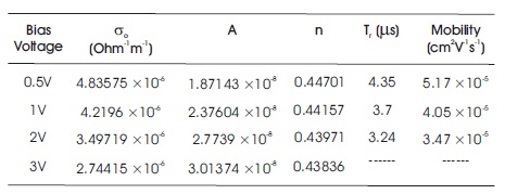
Table 1. Some Conductivity Parameters for ITO/BBPT/Al Device
The observed decrease in the hole mobility of the film with increase in bias voltage is due to the shift of the peak of differential susceptance towards the lower frequency region. This shift is a consequence of increase in rate of relaxation with increasing bias voltage.
Significant information about the conduction mechanism in thin film can be gathered from the study of AC conductivity using dielectric loss tangent (tanδ). The variation of AC conductivity (σac ) as a function of frequency at constant bias voltage of BBPT thin film is shown in Figure 7.
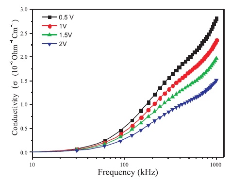
Figure 7. Variation of Conductivity of ITO/BBPT/Al Device with Frequency of AC Signal Applied
The AC conductivity variation obeys the universal power law (Jonscher, 1977; Jonscher, 1983).
where, ω is the frequency, σo is the DC conductivity, 'n' is the power law exponent which generally varies between 0 to 1, and A is the pre-factor which gives the strength of polarizibility. The exponent 'n' describes the degree of interaction between mobile ions with lattice around them, which is expected to increase with decrease in the value of n=1 (for non-interacting system) to n=0. It is observed that the conductivity decreases with decrease in frequency due to the accumulation of charge at the Al/BBPT interface in this device. By fitting equation (3) with experimental data, the values of parameters σo, A, and n so obtained are given in Table 1. The values of 'n' are in good correlation with the theory of hopping conduction in amorphous materials (Pollak & Geballe, 1961; Jonscher, 1977). With the increase in frequency, the hopping between the charge centers and electrodes increases, which results in a sharp increase in AC conductivity. It is also observed that the values of parameters 'n' and σo decreases with increase in bias voltage. This is due to the increase of polarizability strength 'A' with increase in bias voltage which in turn decreases the conductivity of these films. The value of 'n' also indicates non-Debye type relaxation process in these films (Jonscher, 1977). Hence the interactions between the dipoles cannot be neglected and these interactions increases as the DC biasing voltage is increased (value of 'n' decreases with increase in DC biasing voltage).
Organic material 3,5-Bis (4-tert-butylphenyl)-4-phenyl-4H- 1,2,4-triazole (BBPT) is studied for surface morphological and optical characterization in thin film configuration and frequency dependent electrical characterization in ITO/BBPT/Al device configuration. Amorphous morphology, high electrical conductivity, high carrier mobility along with transparent response to the visible light in thin film configuration are the important outcomes of these studies, which indicate that BBPT is a promising ETL material. The conductivity parameters are in good correlation with the theory of hopping conduction in amorphous materials. All these characteristics are among the basic necessities of an electron transport material for optoelectronic device. So, it is concluded that BBPT can be used as an electron transport layer with some suitable emissive/absorbing material to fabricate an efficient Optoelectronic device.
The authors would like to acknowledge Material Science Research Lab, Department of Physics, Guru Nanak Dev University, Amritsar, India for providing the necessary equipment and facilities to carry out this work.