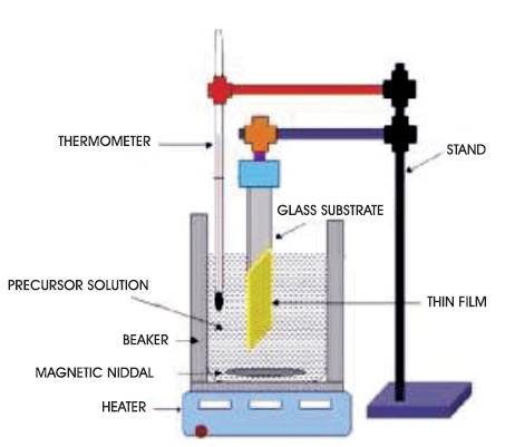
Figure 1. Chemical Bath Deposition Setup
A very simple and economic chemical bath deposition method has been used here for the synthesis of CuInS2(CIS) thin films on glass substrate at 45oC. The purpose of the present work is to synthesize a thin film of CuInS2 , which must have high absorption coefficient in the visible range, high value of photoconductive gain which increases the mobility and life time of charge carriers, and can be used as a hetero-junction in solar cells or photovoltaic devices. The synthesized sample is characterized with X-ray Diffractometer (XRD), Scanning Electron Microscope (SEM), Energy Dispersive X-rays (EDX), and Ultraviolet Visible Spectrophotometer (UV-VIS). The synthesized film is having chalcopyrite structure. Lattice constants, a=5.517 Å and c=11.11 Å, have been obtained which matched well to the reported values. Synthesized particles are spherical in shape and agglomeration of particles can be viewed clearly in SEM images. The chemical composition of the synthesized film of CIS has been analyzed by using Energy Dispersive X-Ray Analysis (EDAX). The transmittance of the deposited film is high between 600-650 nm (visible region). The value of absorption coefficient is found to be in the order of 105 cm-1 in the visible region. Photoluminescence spectrum (PL) is recorded by exciting the sample at 450 nm between 300-900 nm. A strong emission peak is obtained in 620 nm (Red band emission) in the IR region. The dark current varies linearly with voltage. The photoconductive gain obtained for the synthesized sample is ~104.
In recent times, I-III-VI2 type semiconductors have come into sight as most appropriate material for photovoltaic applications. They can be used in areas, including energy conversion, sensing, electronics, photonics, and biomedicine. CuInS2 is one of the semiconductors which crystallize in the chalcopyrite or sphalerite structure (Ortega-López and Morales-Acevedo, 1998). It has direct band gap of 1.5 eV, high absorption coefficient 105 cm-1 (Pathan and Lokhande, 2004) and good stability for solar radiation. In environmental point of view, CuInS2 does not contain any toxic constituents that make it suitable for terrestrial photovoltaic applications (Krunks et al., 1999). Thin film solar cells are having many advantages than silicon-based solar cells; such as lightweight, low cost, flexible, and could be used on the curved surfaces of many buildings and instruments, which makes it a main and promising development direction of future solar energy application. Many researchers have reported the synthesis of CuInS2 thin films by various methods. It includes reactive radio frequency magnetron sputtering (Liu and Shao, 2007), co-evaporation (Gossla et al., 2001), ion layer gas reaction (Qiu et al., 2005), wet chemical process (Guha et al., 2003), spray pyrolysis (Sebastian et al., 2009), Chemical Vapour Deposition (CVD) (Harris et al., 2003), electro deposition (Yukawa et al., 1996), molecular beam epitaxial growth (Niki et al., 1997), and chemical bathing method (Chang et al., 2009). This paper reports the preparation of CuInS2 thin film by using Chemical Bath Deposition (CBD) and its characterization by using various techniques. The objective of the present work is to synthesize an economical and high absorption coefficient film of CuInS2 which can be used in photovoltaic cells or solar cells and increases the efficiency as well.
Chemical Bath Deposition (CBD) technique is a low-cost method, for producing uniform, adherent and reproducible films. It is well known that depending on the deposition condition “ion-by-ion” growth process results in compact and adherent films while a “cluster-by-cluster” process, or colloidal growth, yields porous films (Zhu et al., 1996). This technique is based on the controlled precipitation reaction of an insoluble salt. The major advantage of CBD is that it requires only solution containers and substrate mounting devices. The chemical bath deposition includes two steps; nucleation and particle growth. This method depends on bath temperature, pH of the solution, molarities of concentration and on time.
For the synthesis of CuInS2 thin films, a solution of CuCl2 .2H2O (0.5M) and InCl3 (0.5M) have been taken in a beaker. Both the solutions have been mixed uniformly by stirring. Then triethanolamine (TEA) and ammonia (25%) are added into the beaker. Then sulphur source SC(NH2)2 is added to the solution. Stirring was done for 10 minutes in order to obtain uniform and adherent film. The pH of the solution was 10.5 as measured with pH meter. All the solutions have been prepared in double distilled water. The cleaned microscopic glass substrates were then dipped vertically into the solution. The beaker is then kept inside the liquid o bath at 45oC for 1 hour. After 1 hour, the substrates were taken out and washed thoroughly with distilled water and kept for drying in room temperature for 3-4 h. In Figure 1, chemical bath deposition setup is shown.
Figure 1. Chemical Bath Deposition Setup
For knowing the structure of the obtained film, X-ray diffractograms were recorded by using PANalytical X-ray o diffractometer with CuKα (1.540o A). The optical characteristics were determined in the wavelength range 420 to 640 nm using a Elico SL 210 double beam UV-VIS spectrophotometer. The photoconductivity of the synthesized film was done by using rise and decay method. The thickness of the film is measured by using gravimetric method. The thickness of the film is 38.7 μm.
In order to identify the structure of film material, X-ray diffraction technique has been used. Figure 2 shows the o XRD record of CuInS2 thin film synthesized at 45oC. All diffraction peaks corresponds to the chalcopyrite (tetragonal) structure of CuInS2 . After observation, lattice constants, a=5.517 Å and c=11.11 Å, have been obtained which matched well to the reported values for CuInS2 crystal (JCPDS card No: 98-002-8739). The broadening of peaks suggests that the grain size of film is on a nanometer scale. The relationship between grain size and line broadening can be described by Scherrer's formula,

where λ,β and θ represent the wavelength of X-ray source, the full width at half maximum (FWHM) of a peak, and the Bragg angle, respectively. The grain size of CuInS2 thin film was determined to be 40.72 nm corresponding to the prominent peak (112). Also there are two peaks corresponding to Cu1.8 S1 at 2θ =31.8573 and 2θ =37.9602 (JCPDS-98-006-9756). Remaining peaks are of In1S1 (JCPDS-98-008-1340). Thus it can be inferred that the synthesized film is multiphase. The presence of the multiphase is, in general, attributed to a sum of internal origins obeying the thermodynamics of solid solutions, to defect chemistry and thermal gradient which plays an important role (Suhail, 2012).
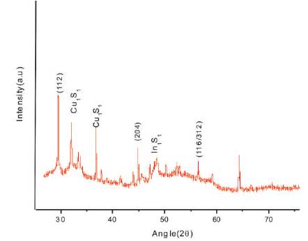
Figure 2. X-ray Diffractogram of CuInS2 Thin Film at 45 oC
In Figure 3, top view of SEM is shown. It is clear that synthesized particles are spherical in shape and agglomeration of particles can be viewed clearly. The film surface appears to be non-uniform. Nanosized particles are seen on the film surface.
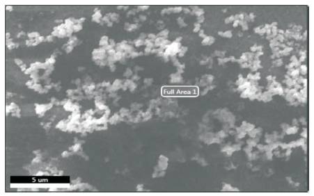
Figure 3. SEM Image of CuInS2 Thin Film
The chemical composition of the synthesized film of CIS has been analyzed by using EDAX as shown in Figure 4. Intense peaks of Cu, In, and S show that the composition consists of Cu, In, and S only. The presence of oxygen was observed. It may be added from the atmosphere (Allouche et al., 2010).
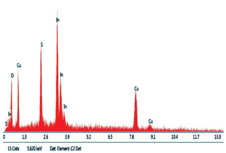
Figure 4. EDAX of CuInS2 Thin Film
UV-Visible absorption spectroscopy is a proficient technique to observe the optical properties of nanomaterials which are directly related to particle size. In Figures 5 and 6, absorption spectrum and transmission spectrum of the film has been shown in the range of 360- 640 nm. The transmittance of the deposited film is high between 600-650 nm (near IR region). Transmittance is low in the ultra-violet region and visible region. It is apparent that the synthesized sample of CuInS2 is having low transmittance and high absorbance in UV and visible regions.
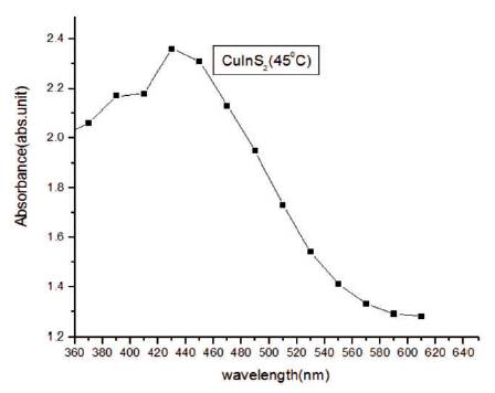
Figure 5. Absorbance Spectra of CuInS2 Thin Film
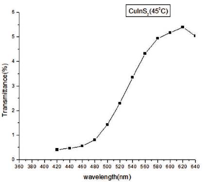
Figure 6. Transmittance Spectra of CuInS2 Thin Film
The band gap energy (Eg) and absorption coefficient (α) of g the synthesized CuInS2 film are determined from the absorption data. The absorption coefficient (α) can be calculated by
where c is a constant (Dehmukh et al., 2012).
The value of absorption coefficient is found to be in the order of 105 cm-1 in the visible region. The high value of makes it valuable for the fabrication of high absorptive layers of solar cell. Plot between (αhν)2 and (hν) is drawn in Figure 7. Thus, the extrapolation of nonlinear plot between (αhν)2 and (hν) gives the value of band gap of CuInS2 thin film as it is a direct band gap material (Tell et al., 1971; Onnagawa and Miyashita, 1984; Nishikawa et al., 1992). The band gap of the film obtained is 2.01 eV. This value is higher than bulk CuInS2 (1.53 eV). A blue shift of 0.48 eV is obtained in comparison to bulk CuInS2 . This increase in the band gap may be associated to smaller particle size showing formation of nanostructure. The levels corresponding to valence band are shifted to lower energy side but levels of conduction band are shifted to higher energy side. Using the hyperbolic band model, the optical properties of CuInS2 thin film have been studied. Average particle size has been calculated by using the following equation.
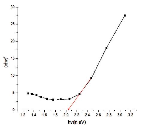
Figure 7. Graph Plotted between (ahv) and hv
where, m is the effective mass of the electron, Egn and Egb are the band gap of nano and bulk samples, respectively. The particle size is in nm range. In Figure 8, a graph is plotted between absorption coefficient (α) and wavelength.
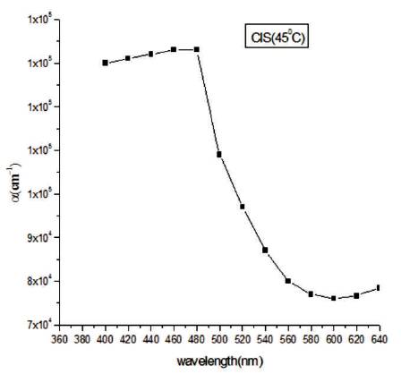
Figure 8. Graph Plotted between a and Wavelength
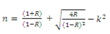
The optical constants n, k, ε1 and ε2, have been calculated at λ=620 nm by using the formula,

and are listed in Table 1.
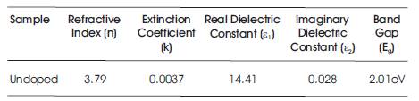
Table 1. The Value of Band Gap, Refractive Index (n), Extinction Coefficient (k), Real and Imaginary Dielectric Constants ( ε1 , ε2) for CuInS2 Thin Film at λ=620 nm
In Figure 9, Photoluminescence (PL) emission spectra of CuInS2 thin film excited at 450 nm is recorded between 300-900 nm. The emission is basically connected with defects which are emerged during the crystal growth. It is related to deformation of crystallinity due to dislocations and vacancies. The photoluminescence process is a charge transfer process, since the photoluminescence emission is associated with the combination of electron from the conduction band, holes in the valence band, and change of the near-band-edge as reported by various authors (Peng et al., 2000; Zhao et al., 2008). A strong emission peak is obtained in 620 nm (Red band emission) in the IR region corresponding to 3.1 eV that has 1180 meV red shift compared to 2.01 eV. This type of red shift may be due to the presence of defect levels in CuInS2 crystal structure (Nose et al., 2009).
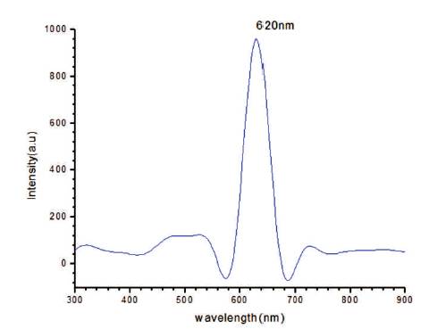
Figure 9. Emission Spectra of CuInS2 Thin Film
In Figure 10, rise and decay curve is shown. When light falls on the sample then photocurrent flows due to photocarriers. Initially photocurrent increases and then it gets saturated. Decay of the current is slow. The photoconductive gain obtained for the sample is ~104 , which is good and can be increased by doping. In Figure 11, a graph plotted between dark current and voltage is shown. Silver has been used for making the electrodes. Voltmeter and ammeter are used for measuring voltage and current by connecting in series. As voltage increases, current increases linearly according to ohm's law. From the dark current study, it is clear that the conductivity of the synthesized film is good.
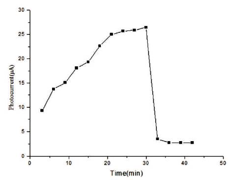
Figure 10. Rise and Decay Curve of CIS Film at 45oC
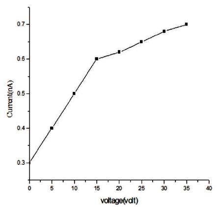
Figure 11. Graph between Dark Current and Voltage
The film of CuInS2 has been synthesized successfully by using chemical bath deposition method on the microscopic glass slides. The synthesized film is having chalcopyrite structure with multiphase. Lattice constants, a=5.517 Å and c=11.11 Å, have been obtained which matched well to the reported values. Surface of the synthesized film is uniform and agglomeration of particles can be viewed clearly in SEM images. In EDAX, intense peaks of Cu, In, and S show that the composition consists of Cu, In, and S only. The presence of oxygen was observed. It may be added from the atmosphere. The synthesized film is nonstichiometric. The transmittance of the deposited film is high near IR region. Absorbance is high in ultraviolet and visible region. The value of absorption coefficient is found to be in the order of 105 cm-1 in the visible region. The band gap of the film obtained is 2.01 eV. This value is higher than bulk CuInS2 (1.53 eV). A blue shift of 0.48 eV is obtained in comparison to bulk CuInS2 . The value of refractive index calculated is 3.79. The imaginary dielectric constant is positive. A strong emission peak is obtained in the IR region corresponding to 3.1 eV that has 1180 meV red shift compared to 2.01 eV. This type of red shift may be due to the presence of defect levels in CuInS2 crystal structure. The dark current varies linearly with voltage. The photoconductive gain obtained for the synthesized sample is ~104 . Thus synthesized film can be used in photovoltaic devices.
Authors are grateful to NIT, Raipur, India for SEM and EDAX. Also they are sincerely thankful to CSIT,Durg and SSGI,Bhilai for providing research facility.
“The authors declare no conflict of interest.”