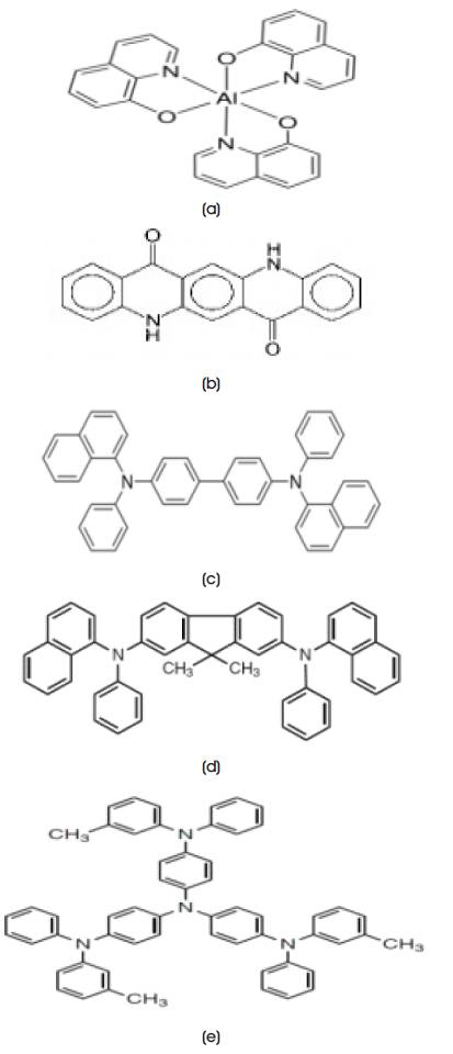
Figure 1. Molecular Structure of (a) Alq , (b) QAD, 3 (c) NPB, (d) DFML-NPB, (e) m_MTDATA
Organic material based Light Emitting Diodes (OLEDs) have greatly dominated solid state semiconductor display technology because of their stupendous features and are accepted world-wide as an emerging trend in the field of display devices. These features of OLEDs introduce low fabrication temperature, low cost, low power consumption, high performance, and flexibility in various applications. This paper demonstrates the performance investigation of fully vertical organic materials based multi-layer OLEDs. For the performance analysis, the extensive comparisons have been performed among the standard three, four, and five layer OLED with their fully vertical device structures by using 4, 4’, 4”– Tris [phenyl-(m-tolyl)-amino]-tri-phenylamine (m_MTDATA) organic material. These impacts are illustrated with the help of performance parameters in terms of current density, luminescent power, and electric field. The complete analysis has been performed by using ATLAS Silvaco numerical simulator. It was found that the concept of fully vertical OLED shows best results in low driving voltage, high current, and high power three layer device applications whereas, four and five layer fully vertical OLED shows best results for high current and low power applications. In three layer fully vertical device, at 18 V the maximum current density obtained was 362.34 mA/cm2 and luminescent power was 0.0185 W/mm. These were raised by 82.07% and 73.18%, respectively when compared with its standard three layer structure. Moreover, in four and five layer fully vertical OLED, current density increases, but luminescent power diminishes due to its electric field effects.
From the past few decades to the present scenario, OLEDs have proven their incredible features in organic electronics, such as high intensity, high brightness, high contrast, high current density, high luminescent power, easy fabrication, low power consumption, low operating temperature, and low cost, which empowers it for the next generation solid state lighting applications ( Helfrich and Schneider, 1965; Tang and Van Slyke,1987; Geffroy et al., 2006; Kaushik et al., 2016, Kumar et al., 2014a, 2014b ). However, to further increase the brightness and to reduce the cost of OLED for large area applications it is required to explore and expand different device structures and to improve the synthesis process of new materials with high accuracy. It has been concluded that white and blue phosphorescent organic light‐emitting diodes have gained almost 100% internal quantum efficiency ( Williams et al., 2007; Su et al., 2008). For the enrichment of OLED performance, scientists have researched and developed multilayered structures from bi-layer structures in the past few years. Multilayered structures showed superior performance over bilayer and single layer OLEDs. As in multilayered device structures the contribution of various layers are different and unique, like Electron Injection Layer (EIL) and Hole Injection Layer (HIL) are used to increase the injection of charge carriers from electrode to internal part of the device, Electron Transport Layer (ETL) and Hole Transport Layer (HTL) are used for proper transportation of carriers from their respective injection layers emissive layer. When a charge carrier reaches to the emissive layer, they recombine on the basis of their mobility and electric field distribution of the recombination zone to illuminate light. Due to such specialized introduction of layers, the recombination rate and electric field in multilayered OLED has increased which enhanced the current density and luminescent power by 9 and 10 times, respectively when compared with bilayer OLEDs (Uniyal and Mittal, 2016).
Previously researchers have demonstrated the impact of quasi vertical and fully vertical based structures in PIN diodes, which has greatly augmented the performance of those devices ( Zou et al., 2016; Zhang et al., 2017). This work, for the first time represents the effect of fully vertical OLED using m_MTDATA material in its three, four, and five layer device structures. By the complete investigation, it was found that the benefits of fully vertical m_MTDATA OLEDs are low driving voltage, high current density, high luminescent power, and high integral flexibility.
In this section, device specification, materials and methodology used for the study has been described.
The device structures engineered for the complete investigations are A, B, C, D, E and F as described below.
where ALq3 - Tris (8-hydroxyquinolinato)aluminium, NPB- N,N’- Di(1-naphthyl)- N,N’- diphenyl- (1,1’-biphenyl)- 4,4’- diamine, ITO- indium-tin-oxide and QAD- quinacridone.
Figure 1 portrays the molecular structure of different materials used in devices A-F. Tris-(8-hydroxy-quinoline)- aluminum (Alq3) works as an Electron Injection Layer (EIL) in devices A, B, and C as it possess properties, such as high electron mobility, astonishing chemical stability, and great luminance yield. However, as explained by Jan Blochwitz (Blochwitz, 2001), chemically unbalanced positive charged state is one drawback of Alq3 . Thus, QAD (quinacridone) doped in Alq3 on a whole serve as a host layer for creating a device more effectual at low cut-involtage. A particular type of material 4, 4', 4”– Tris [phenyl- (m-tolyl)-amino]-tri-phenylamine (m_MTDATA) which has wide band gap energy is employed here as HIL. This will prevent the movement of electron from cathode to conduction layers and also escalates the amount of hole injection from positive electrode to Hole Transport Layer (HTL). NPB and its derivative DFML-NPB are the most favored material used for HTL as they create even morphological device having long lasting age. Anode used in these devices comprises of indium-tin-oxide (ITO) material and this is to be kept in mind here, according to the fabrication laboratory the ITO materials should be exposed in air for 48 hours leading to large work-function of 4.83 eV (Deng et al., 2014). Cathode used for devices A, B, and C exhibit the work-function of 3.343 eV, whereas for devices D, E, and F work-function of 2.343 eV are taken in order to maintain the same difference between negative electrode workfunction and Lowest Unoccupied Molecular Orbital (LUMO) of the ETL (for three layer device) / EIL (for four and five layer devices).
Figure 1. Molecular Structure of (a) Alq , (b) QAD, 3 (c) NPB, (d) DFML-NPB, (e) m_MTDATA
All the simulations have been performed with the help of ATLAS SILVACO simulator tool. Shockley-Read-Hall model has been employed for the proper investigation of active carrier lifespan. Augur and Poole-Frenkel mobility model was used with the amalgamation of Langevin Recombination model for the intensive study of direct recombination in the device working procedure. In order to specify the dependence of high electric field at carrier saturation velocity, among numerical models, Field Dependent Mobility Model (FLDMOB) has been utilized.
All the device structures under study are shown in Figures 2- 4. All are simulated edifices by SILVACO ATLAS. Various device specifications are shown in Table 1.
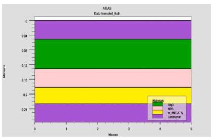
Figure 2. Simulated Edifice representing Device A
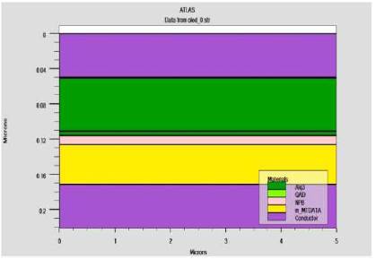
Figure 3. Simulated Edifice representing Device B

Figure 4. Simulated Edifice representing Device C

Table 1. Device Specifications
The designing and simulation of the device has been done by using numerical TCAD ATLAS simulation tool. As per the simulation study, all the equations of the system are solved by using Newton’s numerical technique as it shows quadratic convergence for intensely coupled system equations. This section has been further subdivided for the comparison of the study.
The comparison of current density versus anode voltage characteristics among devices A, B, and C is vividly exemplified in Figures 5 and 6. From the graph it was found that current density of device C was 12.3 times superior than device A and 1.8 times superior than device B.
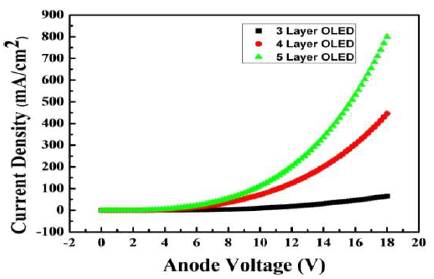
Figure 5. J-V Characteristics contrast among Devices A, B, and C
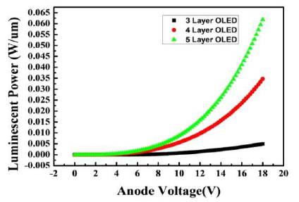
Figure 6. Luminescent Power versus Voltage Characteristics contrast among Devices A, B, and C
Also, luminescent power of device C is 12.46 times greater than device A and 1.78 times greater than device B. The reason behind these outstanding characteristics of device C is its high electric field and faster recombination of charge carriers as given in Table 2.
 >
>
Table 2. Electric Field and Recombination Rate of Devices A, B, and C
For the first time, fully vertical OLED has been introduced which is showing a surprising characteristics that should be taken under consideration for designing and simulation of organic light emitting diodes. The device structures of D, E, and F incorporates fully vertical m_MTDATA, however other models were used by devices A, B, and C. When device A (three layer OLED) is compared with its fully vertical structure made up of m_MTDATA material (device D), it was found that both current density and luminescent power of device D was augmented by 82.07% and 73.19%, respectively at 18 V than device A, as shown in Figures 7 and 8.
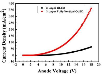
Figure 7. J-V Characteristics contrast between Devices A and D
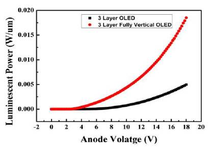
Figure 8. Luminescent Power versus Voltage Characteristics contrast between Devices A and D
The J-V (density-voltage) characteristics and luminescent power output of devices B (4 layer OLED) and E (fully vertical 4 layer OLED) has been clearly illustrated in Figures 9 and 10. From the graph it can be depicted that current density of device E is significantly increased by 71.76% at 18 V when compared with device B.
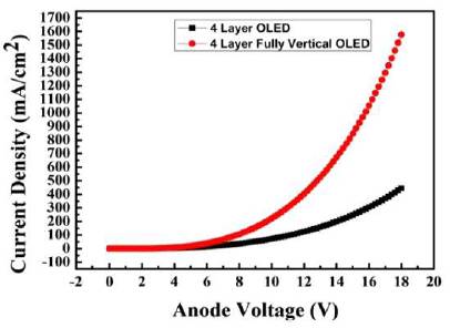
Figure 9. J-V Characteristics contrast between Devices B and E
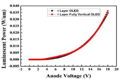
Figure 10. Luminescent Power versus Voltage Characteristics contrast between Devices B and E
Further when the luminescent power of both the devices was investigated, it was found that for lower voltages, i.e. (2.5 V-9.5 V) luminescent power of device E enhances minutely than device B, but for higher voltages (> 9.5 V) it starts degrading when compared with device B.
Now, by increasing the number of layers in OLED structure, the effect of fully vertical design has been demonstrated. It can be seen from the pictorial representation that the current density of device F (fully vertical 5 layer OLED) was amplified by 43.32%, but the luminescent power was lessened by 81.76% at 18 V, when compared with device C (5 layer OLED) as shown in Figures 11 and 12.

Figure 11. J-V Characteristics contrast between Devices C and F

Figure 12. Luminescent Power versus Voltage Characteristics contrast between Devices C and F
As per the discussion of various device structures, it is worth to mention here that the fully vertical OLED is emerging as one of the promising solutions for the future display devices. So, this study could be further recommended for its practical implication and to the fabrication levels for the authentication of the facts, as it can be easily adopted by the manufacturers.
The idea of fully vertical organic material based OLED has been encapsulated by considering three, four, and five layered device structure. This concept of fully vertical structure not only optimizes the value of current density, but also simultaneously improves the luminescent power by significant amount in three layer device. Thus, for three layered devices fully vertical concept should be applied for much higher performance. Consequently, for four and five layer devices demonstration has been done, by which it can be clearly concluded that for high current and low power applications they can be used. These advanced structures could be suggested for the performance enhancement of OLEDs in the near future, depending on the applications.
Authors would like to offer their sincere gratitude to all the members of Research Laboratory and the Department of Electronics and Communication Engineering, Madan Mohan Malaviya University of Technology Gorakhpur (U.P., India) for providing the tool and overall support during the work.