Table 1. Properties of Coating Materials (Callister & Rethwisch, 2007)
Thin film coatings have become an intensively research area for applications related to solar, sensor technologies, and some of the optical applications. The deposition of metallic thin films is mainly carried through DC magnetron sputtering process. The deposition of metallic thin films mainly depends of the process parameters, such as RF power, DC power, and Argon gas flow rate. To obtain the effects of process parameters, L orthogonal array are used. 410- Solar Visible / NIR 9 Spectrophotometer are used to estimate solar absorptance, reflectance, and mirror assessment. These are typical test methods for the measuring solar absorptance, solar reflectance, and transmittance of materials. 410-Solar measures reflectance ta seven sub-bands in 300-2500 nm spectral regions. ET 100 emissometer measures directional reflectance o o at six bands in the thermal infrared spectral region at two incident angles 20 and 60 . Hence, Nano structured thin films are exhaustively used in the area of solar selective coatings.
The need of renewable energy will fullfill the demand of world's energy consumption. The release of CO2 and other pollutant gases are not only harming to the environment, but also human health as well. The production of thin films will enhance to the contribution of energy consumption in the world with an alternative solution to the problem of global warming. The production of thin films has the application potential in window glazing coatings to construct smart windows, solar heaters, solar water heaters, and solar driers (Kanu & Binions, 2009). A thin film is defined as a low-dimensional material created by condensing, one-by-one, atomic/molecular/ionic species of matter. Thin film materials are deposited on substrates, such as glass, plastic or metal, the selection of substrate depends primarily on the application. Presently, most of the research have been carried on the deposition of metal and dielectric thin films for solar energy applications. Thin film materials that are typically used in CSP systems are aluminium, nickel, copper, titanium, tungsten and molybdenum because of their optical and mechanical properties. In recent years, the chromogenic materials were used whose optical properties change according to temperature (thermochromic), external voltage (electrochromic), and radiation photochromic. A study was done on the various deposition processes and parameters typically used in the deposition of aluminium, Nickel, Copper, SiO2, Si3N2, and alumina thin films (Wasa, Kanno, & Kotera, 2012).
The purpose of the paper is to report basic technology behind the deposition and the application of multi-layered nanostructured thin films. This paper also emphasis on the sputtering deposition technique, vacuum technology, process parameters for deposition, and light interaction on the thin films for optical reflectance.
The present work emphasis on composition of the W-Al2O3 thin film coating material, processing conditions, microstructure, and surface finish, influences of the solar absorptance and thermal emittance behavior of these coatings. The response of these nanostructured thin film coatings have been characterized using UV-VIS-NIR spectrophotometer along with integrating sphere in the wavelength range of 250-2500 nm. The absorptance and emittance of 250-400 nm thick metallic coatings on glass and metallic substrates have been evaluated. Tungsten (W) and Alumina (Al2O3) coatings have been deposited using DC and RF magnetron sputtering process.
It was also vital to assess the different techniques usually adapted to promote the longevity of the coatings on polycarbonate, glass substrates. The properties of the coating materials are tabulated in Table 1.
Table 1. Properties of Coating Materials (Callister & Rethwisch, 2007)
The discussion on thin film materials for solar thermal applications, processing conditions, and coating characteristics leading to a comprehensive understanding of the subject related to research work and to identify areas, which needs to be addressed have been studied.
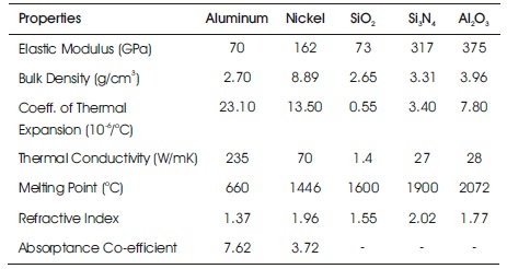
Correa, Almanza, Martı́nez, Mazari, and Cheang (1998) have constructed soda lime glass mirrors with aluminium first layer followed by SiO2 as protective layer using the method of sputtering and reactive sputtering with the help of linear magnetrons. The substrate area was confined to 30 x 60 cm. The parameters considered includes Al target distance and processing pressure variations. In order to get higher reflectance of >90% as shown in Figure 1, it will be necessary to increase the transparency of the SiO2 layer.
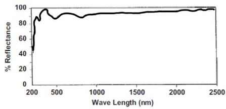
Figure 1. Spectral Reflectance of Aluminum-SiO 2 Multilayer Coatings (Correa et al., 1998)
Moralez and Duran (1997) have studied the usage of sol-gel process for protecting front surface Ag and Al mirrors. SiO2 was used as the protective layer with a thickness of 100-200 nm for this purpose. The mirrors were dipped in the compound for this process. Reflectance values of 85% and 95% were thus obtained for aluminium and silver respectively. Thermal stability of up to 300 oC was achieved with the help of this coating. The method of production is not complex and the cost is cheap as well. The silica coating protects the mirror against environmental damage. Also, these mirrors have lower weight, thus making them viable for them for increased commercial use.
Beegan, Chowdhury, and Laugier (2004) have investigated on two kinds of films- aluminium and tungsten on glass with a systematic variation in film thickness and substrate characteristics. The resulting data were analysed in terms of load-displacement curves and various comparative parameters, such as hardness, Young's modulus, unloading stiffness, and elastic recovery. The results showed how the composite hardness and Young's modulus are different for different substrates, different films, and different film thicknesses. It was found that for a soft film on a hard substrate, the hardness decreases at a small indentation depth. It then kept a constant value, after which increased with increasing indentation depth. This was noticed especially when the indentation depth is equal to or larger than the film thickness.
Ghasempour and Rozati (2011) have studied black nickel coatings deposited on brass, copper, and steel substrates by electrodeposition method. The coatings had good adhesion and thermal stability, with high absorption coefficient depending on the microstructure of the coatings. The highest absorption is for layer deposited on brass without bright nickel and low absorption spectrum associated with the nickel coating on steel with bright nickel middle layer and the absorptance of ~76% was observed as shown in Figure 2.
Figure 2. Absorption Spectrum of Black Nickel on Brass, Copper and Steel Substrates as a Function of Wavelength (Ghasempour & Rozati, 2011)
Khalifa, Al Hameda, Shoeib, Mohamed, and Ahmed (2015) have studied black electroplating nickel coatings, which are electrodeposited. The measured reflectance was 55% in the wavelength range of 250-550 nm. The absorption percentage range was 99.45% in the wavelength range of 250-550 nm. Carter, Walde, McDonough, and Roche (2002) have studied the deposition of alumina on glass substrate using reactive sputtering process, high purity aluminium target in combination with RF inductively coupled plasma as been used as source of oxygen ions. The deposited films were characterized using spectrophotometer. Results showed that with increasing oxygen flow, the transmittance also increased. They reported that high density of oxygen ions is essential for achieving transparent alumina thin films. Vila, Caceres, and Prieto (2003) have deposited silicon nitride thin films by reactive sputtering using a range of Ar/N2 sputtering gas mixtures. The hardness and the Young's modulus of the samples were in the ranges 8-23 and 100- 210 GPa, respectively. The reasons for large variation in hardness and Young's modulus have been attributed to bonding, atomic concentrations, and structure of the films. Reddy et al. (2014) have sputtered samples of aluminium to study transmittance characteristics of the thin film. Optical characterization was performed on the samples. The results showed zero transmittance in optical and IR ranges. Characterization of the same was performed using nano indentation technique, which yielded a hardness value of 6 GPa and Young's Modulus of 116 GPa.
The thin film processing techniques (Correa et al., 1998) are broadly categorized into physical and chemical vapour deposition systems as shown in Figure 3.

Figure 3. Methods of Thin Film Deposition Techniques
The deposition process of a film can be divided into three basic phases:
Chemical and Physical vapor deposition processes are widely used to deposit thin films, atoms in the vapor form are transported through a vacuum or low pressure gaseous (or plasma) environment to the substrate, a layer is formed upon condensation. Physical vapour deposition processes are used to deposit films, Physical vapour deposition processes with wide range of thicknesses are used to produce multilayer coatings. Material of target, Power supplied to magnetron either DC or RF, Argon gas flow rate and distance between target and substrate are the process parameters on the deposition rate of thin films sputtered using magnetron sputtering. Deposition rate of thin films are varied by the variation of argon gas flow rate. Higher deposition rate and higher infrared reflectance in the IR range will attain by the increase of argon gas flow rate.
Thin films mainly deals with progress of vacuum technology and systems adept of reaching pressures proper for emergent uniform films at rational deposition rates. Thin film coating materials are crucial components of continuous technical advances arranged in the field of photonic, magnetic, and optoelectronic devices. The refinement of resources into thin films permits simple amalgamation into several kinds of devices. Properties of material considerably change while evaluated in the variety of thin films. Most of the capable materials are relatively utilized in thin film form due to their specific optical, magnetic, electrical properties, and wear resistance. In the process of depositing thin films, it is essential to consider that the properties of thin films that can be altered by differing thickness parameter.
Most thin film deposition and processing methods employed to exemplify and quantify the properties of the films require a vacuum or some port of decreased-pressure environment. A vacuum can be stated as volume encompassing less gaseous molecules compared to surrounding environment when both containing similar matter at same temperature. It offers a long Mean Free Path (MFP) for collision involving vaporization basis and the substrate. Empirical formula to calculate mean free path is shown in equation (1) (Petrov, Barna, Hultman, & Greene, 2003).
where P is the pressure in mbar.
Vacuum are often categorized as one of four main types as shown in Table 2.
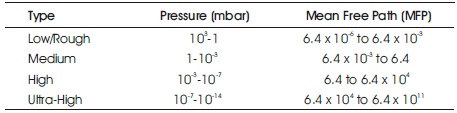
Table 2. Vacuum Categories (Umrath, 2007)
Sputtering deposition technique is most commonly used method for thin film deposition. Figure 4 shows the sputter deposition method (Callister & Rethwisch, 2007). In this method, particles are ejected from target source and get deposited on substrates such as silicon wafer, SS304, glass, and polycarbonate materials. These sputtered atoms possess broad energy distribution normally up to 9.5-10 eV. In processing of thin films, usually argon gas is used as sputtering gas due to higher molecular weight of argon. While sputtering light and heavy elements sputtering gases such as neon and krypton/xenon is preferred. In thin film deposition process, it is essential to scrutinize that for efficient momentum transfer of ions from target to substrate, atomic weight of sputtering gas should be almost equal to atomic weight of target source.

Figure 4. Sputter Deposition Process for Thin Films (Callister & Rethwisch, 2007)
The application of sputter deposition includes fabrication of computer hard disks. Antireflection coatings on glass for optical purposes are also deposited by this method.
When light travels from one medium to another, some of the radiations are transmitted through the medium, some radiations are absorbed and rest of the radiations will be reflected at the interface of the object. The intensity (Io) of the beam incident on the surface of the solid medium must be equal the sum of the intensities of the transmitted radiation, absorbed radiation, and reflected beams denoted as IT, IA, and IR, respectively shown in equation (2) (Callister & Rethwisch, 2007).
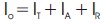
The ratios of intensities are called, transmissivity (IT/I0), absorptivity (IA/I0), and reflectivity (IR/I0). In order to evaluate the optical performance of an candidate reflector materials for solar thermal applications, the two methods of optical testing have to be done. First, the spectral hemispherical reflectance R(λ, θ) measured at the wavelength range of 250< λ <2500
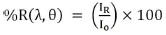
In order to optimize performance of the thin films, wavelength of light, angle of incidence, refractive index, and thickness of layers are varied while designing the thin film. In order to maximize reflection, ideally there should be a 0° phase shift between two reflected portions when they recombine at first interface. To maximize reflection and minimize transmission, the reflected beam must have a constructive interfere with one another. Figure 5(a) shows an illustration of constructive interference. When light moves from a medium of a given refractive index, n1, into a second medium with refractive index, n2, both reflection and refraction of the light may occur.
Figure 5. (a) Constructive Interference (b) Optical Phenomena of Multilayer Thin Films (Hecht, 2002)
Reflection as defined through Fresnel's equation, which provides the amount of reflection that will occur from the refractive index change at an interface at normal incidence of two non-absorbing media of refractive index na and nf is given by equation (4) (Callister & Rethwisch, 2007).
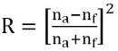
Figure 5(b) indicates the light propagation inside multilayer thin films. At the boundaries, light repeatedly reflects and transmits between films. Light reflects into the medium after multiple refraction and reflection. The reflected and refracted light with particular wavelengths are strengthened or weakened due to their phase differences.
The above equations are suitable for single layer coatings on substrates, schematically shows the complex reflection, refraction, absorption that occurs within the single layer thin film coatings is shown in Figure 6 and Table 3 shows incident, reflected, and transmitted angles of coatings for reflectors and absorbers.

Figure 6. Single Layer Thin Film Coatings Angles (Hecht, 2002)
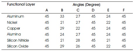
Table 3. Incident, Reflected and Transmitted Angles for Functional Coatings (Hecht, 2002)
The ratio of the radiant flux absorbed by a body to the incident radiation flux on the surface is defined as absorptance. The total absorptance of any media is the absorptance taken over the whole spectrum. Absorptance of a surface denoted A is given by equation (5) (Hecht, 2002).

where φa is the radiant flux absorbed by the surface; φi is the radiant flux incident on the surface. Absorptance depends on the dimensions of the thin film, its density, and microstructure.
As light travels through a component, reflections will occur at the two interfaces of index change on either side of the coating. In order to maximize reflection, ideally there should be a 0° phase shift between these two reflected portions when they recombine at first interface. This phase difference correlates to a λ/2 shift of the sinusoid wave, which is best achieved by adjusting the optical thickness of the layer to λ/4. The reflected beam must be constructively be in interference with one another to maximize reflection and minimize transmission. By manipulating the exact thickness and composition of the layers in the reflective indices, the reflection characteristics can be modified according to particular application. Figure 7 shows an illustration of constructive interference.
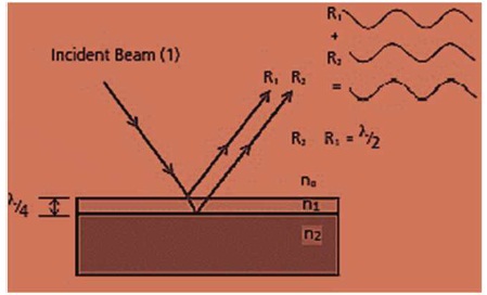
Figure 7. Constructive Interference (Dikshit & Bhatia, 2010)
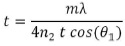
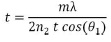
The thickness of the film to achieve constructive interference is given by equation (6) (Dikshit & Bhatia, 2010).
where,
t - film thickness
n2 - the refractive index of the film
θ1 - angle of incidence of the wave on the lower boundary,
m - an integer, and
λ - wavelength of light
As light travels through an optical component, reflections will occur at two interfaces of index change on either side of the coating. In order to minimize reflection, ideally there should be 180° phase shift between these two reflected waves when they recombine at the first interface. This phase difference correlates to a λ/2 shift of the sinusoidal wave, which is best achieved by adjusting the optical thickness of the layer to λ/4. Figure 8 shows an illustration of Destructive interference (Bachman, Chiang, Chu, & Li, 1999).
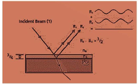
Figure 8. Destructive Interference (Bachman et al., 1999)
The thickness of the film to achieve destructive interference is given by equation (7) (Bachman et al., 1999)
The thickness of the coating materials are calculated by using the equations (5) and (6) for constructive and destructive interference with angle of incident 45o with corresponding refractive indices of the materials. The computed values are given in Table 4.
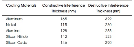
Table 4. Thickness for Constructive and Destructive Interference of Coating Materials (Bachman et al., 1999)
A UV–VIS–NIR Spectrophotometer basically consists of a light source, a monochrometer, a sample compartment, and a detector as shown in Figure 9 (Otto-Schott-Strabe, 2010). The most commonly used light sources are halogen lamps used for the visible and near-infrared regions and the deuterium lamps used for the ultraviolet region. Monochromatic light of different wavelengths ranging from Ultraviolet to Infrared are produced by using either a prism or a diffraction grating as the dispersive element. This monochromatic light is then incident on the sample, the intensity of light reflected or transmitted through the sample is detected. Photomultipliers and silicon photodiodes are typical detectors used for the ultraviolet and visible regions while for the near-infrared region, PbS photoconductive elements or InGaAs photodiodes are being used.
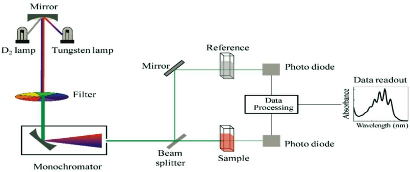
Figure 9. Schematic of a UV-VIS-NIR Spectrophotometer (Ohring, 2001)
Based on the process parameters identified for sputtering, the experiment plan is prepared so that sputtering process is carried out at different conditions to observe effects of these conditions on thin film properties. The experimental plan is achieved on the basis of Taguchi L9 orthogonal array is shown in Table 5 (Montgomery, 2017). Based on the below Table 5, the experimental plan as derived from L9 orthogonal array is represented in Table 6. The various levels for deposition parameters are selected based on consistency of deposition machine. Since the DC Power, RF Power and Argon gas flow rate are process parameters, the experiments are carried out with different combinations to obtain the optimized conditions after characterizing and analysing deposited thin films. Taguchi layout is used in the estimation of percentage effects of each parameters on thin film properties.
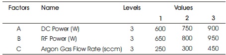
Table 5. Parameters and Levels for Thin Film Deposition Process
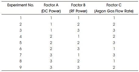
Table 6. Deposition Conditions based on L Orthogonal Array
The different thin film deposition parameters affect the absorptance response to different degrees. The relative amount of the each factor effects can be predicted by using ANOVA. Robust design table for optimization of absorptance of W-Al2O3 thin films is tabulated. The ANOVA results of absorptance are presented in Table 7. From Table 7, it is clear that absorptance responses are analysed for different values of deposition parameters to optimize the process parameters. Also the percentage effects plot are plotted for each of deposition parameters and is shown in Figure 10.

Table 7. Robust Design Table for Optimization of Absorptance of W-Al O Thin Films on SS304 Substrates
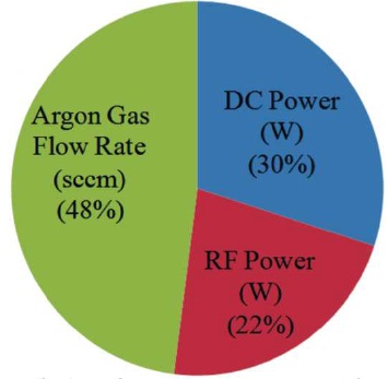
Figure 10. Percentage Contributions of Deposition Parameters on Solar Absorptance of W-Al O Thin Films on SS304 Substrates
It clear from Figure 10 that DC power has 30% of contribution, RF power has 22% and argon gas flow rate has 48% of contribution and is higher among all three deposition parameters. Hence in achieving higher solar absorptance of metal-ceramic thin films, it is essential that argon gas flow rate should be maintained as minimum as possible. While RF power should be maintained high and moderate value for DC power is preferable. Hence from Table 7 and Figure 10, the optimized deposition parameters are DC power to be 750 W, RF power to 950 W and argon gas flow to be 250 sccm to achieve an absorptance greater than 0.75.
Absorptance and emittance are the response features for deciding the optimum coating deposition parameters. Experimental results are analysed to find the effect of deposition factors and their interactions with each other on the absorptance and emittance. 410 solar measures reflectance in seven sub-bands spectral regions. Further SEM, EDAX can be used to characterize the coated samples.
This paper presents sputtering deposition technique for fabricating composite thin film coatings, where Composite thin films deposited by Physical Vapour Deposition (PVD) methods are exhaustively studied from past two decades in order to fulfil increasing demands by coating industry. Robust design table for optimization of absorptance and reflectance are presented to predict the relative effect on each factor were drawn using ANOVA. The optimized deposition parameters are DC power to be 750 W, RF power to 950 W and argon gas flow to be 250 sccm to achieve an absorptance greater than 0.75. The main effect plots, Surface plots, and Contour plots can be used to study the effects on factors. The thin films are characterized to Scanning Electron Microscopy to obtain surface morphology and also EDAX to detect the exact composition of elements. The composite films having metal and an insulator were deposited by using a high -6 vacuum (10 Torr) sputtering process (RF and DC). Hence the sputtering process is versatile and provides good adhesion between the film and substrate. Most commonly used metals for sputtering are Al, Ni, Ti, Mo, Cu, and V. While the dielectric materials are SiO2, Si3N4, and Al2O3. Among these metals, Aluminium is used as non-ferrous metal as it is low cost and has unique set of material properties for applications such as structural components and mirror reflectors.
The authors would like to thank the Science and Engineering Research Board (SERB) Department of Science and Technology, New Delhi, India for funding this research work. The authors also like to thank Department of Mechanical Engineering and management of RV College of Engineering for their support.