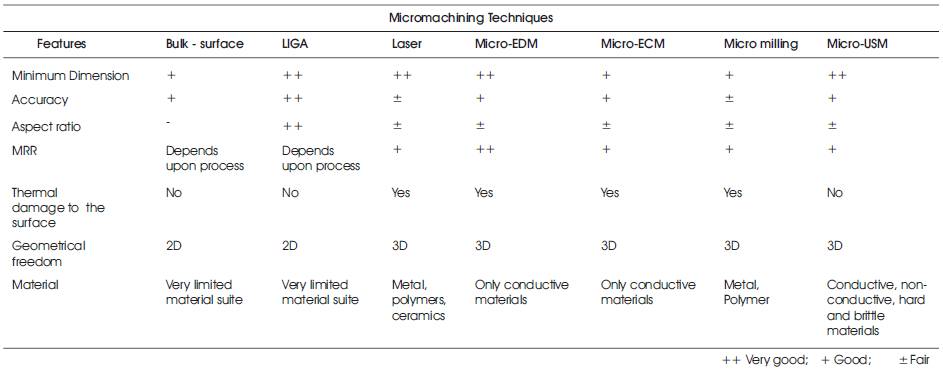
Table 1. Common Attributes of Different Micromachining Techniques [3]
A comprehensive understanding of the materials and their processing helps efficient fabrication of component in micro devices such as microelectromechanical systems (MEMS). Silicon is one of the widely used materials to create many integrated circuits used in consumer electronics in the modern world. Glass and titanium are two other materials widely used in fabrication of MEMS which usually exhibit very high degree of reliability. However, one of the most challenging tasks for MEMS industries is to find new methods for machining such difficult-to-process materials. This paper explores a non-thermal and non-chemical approach to machine these materials using ultrasonic micromachining (USMM). In the current work, microdrilling was carried out on silicon, glass and titanium using USMM. Machinablity aspects while drilling holes have been analysed in terms of study of surface roughness and tool wear. The process yielded a surface finish upto 2.08µm, while the highest tool wear among the attempted materials was observed while machining relatively ductile titanium. The study proves the viability of micro drilling of the target materials with parametric analysis. A brief review of different materials used for MEMS, their suitability and processing challenges has been presented.
Microelectromechanical systems can be conceptualised as miniaturized mechanical and electromechanical elements that are made using microfabrication techniques. In a variety of devices and fabrication process MEMS occupies the size range from 1mm to 1µm. It has already found significant applications in sectors that include, automobile industry, aircraft industry, chemical industry, pharmaceuticals, manufacturing, defence, biomedical and environmental monitoring [1]. A number of applications within these industries contain MEMS technology that needs microdrilling of various parts. The microdrilling required in these elements is a difficult task with the help of conventional microfabrication techniques because of hard and brittle nature of the work material. Silicon, glass and ceramics are the traditionally used materials for the purpose. Silicon is one of the widely used materials to create many integrated circuits used in consumer electronics today. Second widely used material is glass. Metals such as titanium are also used to create MEMS elements and can exhibit very high degree of reliability.
Various non traditional techniques such as micro electro discharge machining (micro EDM), micro Electro chemical machining (micro ECM), laser micro drilling, and silicon micromachining are widely used for microdrilling in these parts [2]. But due to certain limitations, for instance thermal stresses, high cost of equipment, and structure flexibility post a barrier to use these techniques. The standardized fabrication process such as silicon bulk or surface micromachining in MEMS are limited by materials, geometrical limits and fabrication process costs and time. Table 1 presents a comparative analysis among different micromachining techniques. Consequently, ultrasonic micromachining (USMM) is proved to be good for microdrilling in such MEMS materials [4]. USMM is a mechanical material removal process used to erode holes and cavities in hard or brittle work pieces by using shaped tools, high-frequency mechanical motion, and an abrasive slurry. Unlike other non-traditional processes ultrasonic machining does not thermally damage the work piece or appear to introduce significant levels of residual stress, which is important for the survival of materials in service.
Table 1. Common Attributes of Different Micromachining Techniques [3]
A complete understanding of MEMS requires a mature knowledge of the materials used to construct the devices, as the material properties of each component can influence device performance. The paper does not attempt to present a comprehensive review of all materials used in MEMS. It does, however, detail a selection of material categories that are widely used and important in MEMS. Three types of MEMS materials; silicon, glass and titanium were chosen for microdrilling using USMM and a study is presented with respect to the surface roughness characteristics of microdrilled surfaces on said materials.
Silicon is the most widely known semiconducting material in use today. Single crystal Si has a diamond (cubic) crystal structure and like many semiconducting materials, it can be doped with impurities to alter its conductivity. Mechanically, Si is a brittle material with Young's modulus of about 190GPa. Single-crystal Si serves several key functions for MEMS applications. Single-crystal Si is perhaps the most versatile material for bulk micromachining, owing to the availability of well-characterized anisotropic etches and etch-mask materials. Single-crystal Si substrates are used in surface micromachining applications as mechanical platforms on which device structures are fabricated [5]. In the case of Si-based integrated MEMS devices, single-crystal Si is the primary electronic material from which the integrated circuit devices are fabricated. Bulk micromachining of Si uses wet and dry etching techniques in conjunction with etch masks and etch stops to sculpt micromechanical devices from the Si substrate. An anisotropic sidewall profile could also be produced in virtually any Si substrate by deep reactive ion etching, ion beam milling, or laser drilling [6].
The next most common material for the fabrication of surface micromachined MEMS devices utilizes polycrystalline Si (polysilicon) as the primary structural material, silica as the sacrificial material, and Si3N4 for electrical isolation of device structures. Like single-crystal Si, polysilicon can be doped during or after film deposition using standard IC processing techniques. Silica can be grown or deposited over a broad temperature range (e.g., 200 to 1150°C) to meet various process and material requirements. The SiO2 is readily dissolvable in hydrofluoric acid (HF), an IC-compatible chemical, without etching the polysilicon structural material [7].
Polysilicon is an attractive material for surface micromachined structures because it has mechanical properties comparable to single-crystal Si, and also it is resistant to SiO2 etchants. Polysilicon thin films are commonly deposited by a process known as low-pressure chemical vapour deposition (LPCVD) for MEMS and IC applications. This deposition technique was first commercialized in the mid-1970s [8] and has since been a standard process in the microelectronics industry. Polysilicon is made up of small single-crystal domains called grains, whose orientations and/or alignment vary with respect to each other. The roughness often observed on polysilicon surfaces is due to the granular nature of polysilicon.
Another material that has found utility in MEMS is spin-on-glass or silicon on glass (SOG), which is used in IC processing. As the name implies, SOG is applied to a substrate by spin coating. The material is polymer based with a viscosity suitable for spincoating, and once dispensed at room temperature on the spinning substrate, it is cured at elevated temperatures to form a solid thin film. The potential uses of SOG in MEMS have been illustrated in very limited literatures [9-10]. The first example presents a glass reflow process to implement SOG MEMS devices on Si–glass compound substrate with embedded silicon vias [9]. The silicon vias are patterned by photolithography and dry reactive ion etching, and then hermetically sealed by Pyrex7740 after the glass reflow process. The single crystal silicon (SCS) on Si–glass compound substrate is exploited to fabricate MEMS devices. This SOG device with embedded silicon vias is ready for 3D integration with IC. In the second example, high-aspect-ratio channel-plate microstructures were fabricated from SOG [10]. The process required the use of molds to create the structures. Electroplated nickel (Ni) was used as the molding material, with Ni channel plate molds fabricated using a conventional Lithographie, Galvanoformung, Abformung (LIGA) process. The Ni molds were filled with SOG, and the sacrificial Ni molds were removed in a reverse electroplating process. In this case, the fabricated SOG structures were over 100 μm tall. Essentially, the bulk micromachined structures were fabricated using a sacrificial molding material system.
The silicon on glass (SOG) module was developed to integrate CMOS and high-aspect ratio MEMS sensors and actuators. This was accomplished by forming recesses on a glass wafer, anodically bonding a silicon wafer to that glass wafer, and using deep reactive ion etching to etch MEMS devices through the backside of the silicon wafer over the glass recess.
Aluminum (Al) is probably the most widely used metal in microfabricated devices. In MEMS, Al thin films can be used in conjunction with polymers such as polyimide because the films can be sputter deposited at low temperatures. In most cases, Al is used as a structural layer; however, Al can be used as a sacrificial layer as well. The polyimide/ aluminium combination as structural and sacrificial materials, respectively, has also been demonstrated to be effective for surface micromachining [11]. In this case, acid-based Al etchants can be used to dissolve the Al sacrificial layer. A unique feature of this material system is that polyimide is significantly more compliant than polysilicon and silicon nitride (e.g., its elastic modulus is nearly 50 times smaller. Finally, because both polyimide and Al can be processed at low temperatures (e.g., below 400°C), this material system can be used subsequent to the fabrication of ICs on the wafer. Copper, gold, and aluminum are the most commonly used metals in 3D integration and MEMS packaging [12].
Tungsten (deposited by CVD) as a structural material and silicon dioxide as a sacrificial material have also been processed using surface micromachining [13]. In this case, HF is used for removing the sacrificial oxide. In conjunction with high-aspect-ratio processes; nickel and copper are being used as structural layers with polyimide and other metals (e.g., chromium) as the sacrificial layers.
Titanium has a number of properties that makes it more attractive when compared to traditional semiconductor materials such as silicon for certain applications in MEMS. First, and perhaps foremost, as a metal it has inherently higher fracture toughness than silicon. This has obvious implications for enhanced durability and shock-resistance relative to silicon. Titanium also has greater biocompatibility and is suitable for a number of applications, including titanium-based MEMS relays. The bulk micromachining of titanium was demonstrated using the Metal Anisotropic Reactive Ion Etching (MARIO) Process [14]. This process cycles between chlorine-based plasma for the dry etching of titanium and an oxygen plasma for sidewall passivation, resulting in an anisotropic deep etch with vertical side walls.
Study of many of these material systems has been either limited or is in the preliminary stages; as a result, their benefits are yet to be determined. The used standardized fabrication process such as silicon bulk or surface micromachining in MEMS can precisely perform 2D machining at the micro level, that is, they can machine thin films extremely well. However, they are unable to produce 3D components with high aspect ratio. These techniques also suffer from limitations such as restricted materials choice, inability to produce complex profiles, and huge investment for facilities and equipment. In the present work, investigation on ultrasonic micromachining of three widely used materials for MEMS applications, whose processing is considered challenging at the micro domain, silicon, glass and titanium have been presented.
In USMM, the removal of material is accomplished by the abrading action of grit-loaded slurry, circulating between the workpiece and a tool. The contributing mechanisms in USMM can be summarized into four categories as [15-17] (i) Micro chipping by impact of the free moving abrasive particles (ii) Mechanical abrasion by the abrasive particles against the work piece surface (iii) Cavitation effects in liquid agitated by ultrasonic vibration (iv) Chemical actions associated with the liquid being employed. However, individual contribution of each mechanism is yet to be ascertained.
In USMM, the tool is vibrated at small amplitude and high frequency, typically 10–20 µm at 20–50 kHz. Figure 1 illustrates the schematic of a basic set-up of an USMM which includes the horn-tool assembly, the generator, and the slurry supply unit. The sonotrode or horn-tool assembly consists of a transducer, a booster and a horn. The electronic generator powers the transducer, creating impulses that occur at a range of 19.5 to 20.5 kHz, and automatically adjusts the output frequency to match the resonant frequency of the tool, which varies according to the horn shape and material [18]. The transducer converts the electrical pulses into vertical stroke. This vertical stroke is transferred to the booster, which may amplify or suppress the stroke amount. The modified stroke is then conveyed to the horn-tool assembly [19]. The amplitude along the face of the tool typically falls in a 10 to 20 μm range. The vibration amplitude is usually equal to the diameter of the abrasive grit used. The slurry system supplies slurry of water and abrasive grit, usually silicon/boron carbide, to the cutting area. In addition to providing abrasive particles to the cut, the slurry also cools the horn and flushes away the debris from the machining zone and refills the gap with fresh slurry. The operator controls provide inputs for manual or automatic sequencing of operations. Controls include variable static load, frequency and amplitude variation, table position, speed control of the ram movement, cycle timing, and flush timing.
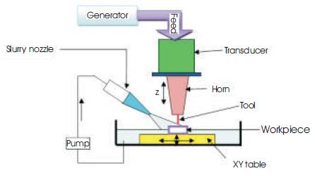
Figure 1. Schematic of an USMM
A 4 mm thick plate of each glass, and Ti were employed as workpiece materials for the ultrasonic drilling trials. Silicon with 500 µm thickness was also used for conducting the experiments. Table 2 shows structural and mechanical properties of the workpiece materials.
The USM experiments were carried out in a stationary Sonic- Mill machine (AP-500) with a power output of 500 W (Figure 2). The power supply is equipped with automatic frequency control and automatic load compensation providing constant output amplitude at desired setting to meet the different energy requirement encountered during the operation cycle. An electrostrictive PZT transducer converts the electric oscillations into mechanical vibrations in the frequency range of 20 kHz. A 20% power rating was used during the experiments. The static load applied on the horn was constant throughout the experiments. The abrasive slurry was made with silicon carbide (SiC) with mean grain size of 24 μm (350 mesh) and water in the ratio 1:3 by weight. A stainless steel solid tool having a circular cross section with 450µm diameter and 5 mm in length was used as cutting tool. The material removal rate (MRR) was determined by measuring the time spent to machine a given depth (d) in several stages of machining. The value of d was set between 4mm and 500μm depending on the availability and machinability of the workpiece. Measurements of tool wear ratio as a function of drilling depth were performed on the said materials. The tool wear ratio can be defined as the length of tool wear to the depth of the hole. Scanning electron microscopy (SEM) (FEI Quanta 200 FE-SEM, Czech Republic) was employed to characterize the micromechanisms related to material removal under ultrasonic abrasion condition. Surface roughness values were assessed using an optical profiling system (Veeco, Model WYKO Nt1100).
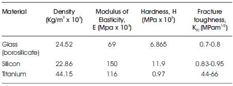
Table 2. Mechanical Properties of Workpiece Material
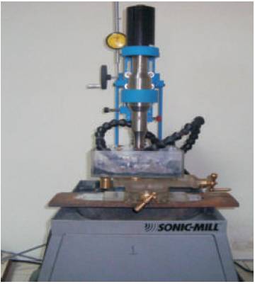
Figure 2. Experimental set-up of an USMM
Figure 3 illustrates the variation of the MRR as a function of the cutting depth (d) for the three workpiece materials investigated. Two different behaviours have been observed in the MRR Profile. In the case of titanium, MRR decreases with d drastically upto a hole depth of ~250 μm. However, in case of glass and silicon, MRR decreases with d at a significantly high rate upto 1000 μm and 200 μm respectively. Afterwards, it remained almost constant and seemed to be independent of d. Decrease in MRR with increasing d, is usually explained by the insufficiency in recycling abrasive particles at the machining interface because of accumulation of the debris. The recycling capacity affects the hammering and impact actions of the abrasive particles in the working gap. In addition, the problem with slurry turbulence probably increases with d causing a decrease in the MRR.
The decrease in MRR with d was not observed for all the materials investigated; thus, it is reasonable to suggest that such behaviour is much more influenced by the inherent properties of the workpiece material than to any operating parameter. Considering the properties listed in Table 2, it is noticed that the main difference between the two groups of materials is in its hardness. It is observed that the hardness of titanium is significantly less (~(1/7) of glass, and ~(1/12) of silicon) than the other two materials discussed here. Therefore, it behaves more like a ductile material and after cutting through a certain value of workpiece thickness in which the basically the impurity and oxide layer is removed, the cutting performance decreases sharply.
Further, the abrasive particles loose its cutting power because the impact energy of the abrasive particles is being absorbed by the relatively ductile material (Ti) itself. It must be noted that the titanium used in the work has approximately fifty times higher toughness than the other two materials (Table 2) which help it to absorb more energy. Further, the impinged particles might also get embedded into the soft ductile phase causing a rapid slowdown in the MRR.
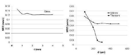
Figure 3. Typical MRR profiles as a function of cutting depth
Figure 4 shows the percentage tool wear while machining different work materials. In the present work, tool wear ratio was evaluated for the purpose of analysis. In general, tool wear ratio is defined as the length of tool wear to the depth of the hole. It was found that, the tool wear ratio is maximum in case of titanium. The reason for the observed result is attributed to the intrinsic properties of the material. As abrasive particles don't cut the workpiece after a certain value of workpiece thickness, they start accumulating at a depth. Thus the abrasive grain causes the local deformation at the tool working area, followed by the crack generation and material spalling from the tool, leading to the tool wears. Tool wear can also be affected by toughness of the material.
Figure 5 (a) & (b) illustrates typical SEM micrographs of ultrasonically machined surfaces of glass and silicon respectively. It can be observed that there is absolutely no plastic deformation and brittle microcracking is the dominant material removal mechanism connected with the ultrasonic abrasion of hard and brittle material. The irregularities showed on the sidewall surface of the drilled hole are because of the relatively higher size of the abrasive particles with respect to the machining dimension and straying abrasive particles getting deflected by the impact of the tool edges rather than the bottom of the tool end. This results in higher roughness in the proximity to the hole entry. The ripples on the surface showing the fatigue fracture on the surface and result in larger pits than the particle size involved. The roughnesses due to stray cutting action of the abrasives are observed to be similar in both glass as well as silicon (Figure 5). The surface roughness was measured on the machined hole surface. The surface roughness for the machined hole in case of silicon is depicted in Figure 6, the mean surface roughness is observed to be 2.08µm. The resulting roughness can be minimized by precisely controlling various process parameters and using submicron abrasive particles. A very high Rt value, on the other hand, indicates presence of localized microcrack associated with brittle fracture of the material. The localized crack (higher value of Rt) is contributing towards observed high value of Ra. The machined surface morphology, otherwise appears uniform (Figure 6).
In case of titanium a ring type burr formation was observed. As the abrasive slurry approaches the surface of the workpiece, a bulge begins to develop on the surface of the workpiece. This burr initiation stage begins with local plastic deformation because of the relatively ductile nature of the workpiece. After burr initiation, the bulge continues to develop and enlarge, Figure 7. The burr development in drilling of titanium indicates the transition from cutting to ploughing.
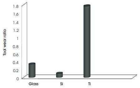
Figure 4. Tool wear ratio of different materials
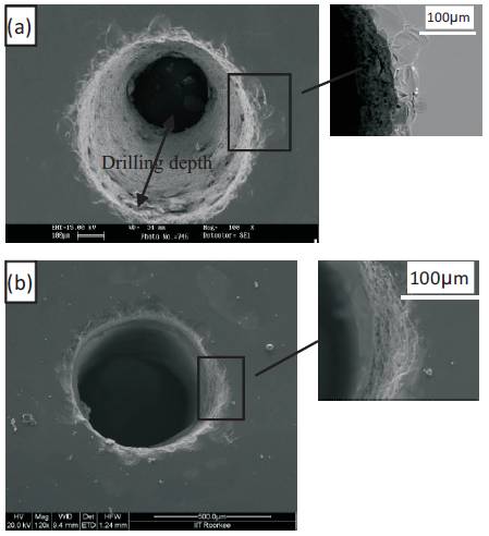
Figure 5. SEM micrographs of ultrasonically machined surfaces of (a) glass(b) silicon with solid tool; insets: Zoomed view of the irregularities on the surfaces
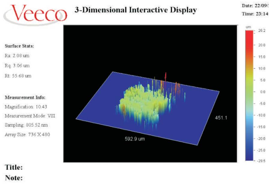
Figure 6. A typical 3D surface roughness map of silicon
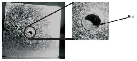
Figure 7. Microdrill in titanium, inset: Zoomed view of the microhole
A brief review of different materials used for MEMS, their suitability and processing challenges has been presented. The early development of MEMS can be accrediting to the recognition of silicon as a mechanical material but the rapid expansion of MEMS is due in part to the inclusion of new structural materials that have expanded the functionality of microfabricated devices. Preliminary micro USM trials were carried out on different brittle and hard materials revealed the influence of structural and mechanical properties of workpiece materials on the rate of material removal and the topography of machined surfaces. The rate of material removal decreases with increase in machining depth in all the three materials owing to increased congestion in the machining zone due to the debris produced. However, rate of material removal decreases sharply in case of titanium which is relatively tougher than the other two materials attempted. Under these circumstances, abrasive grits lose their cutting power more quickly because of absorption of impact energy. Tool wear ratio is maximum in case of titanium owing to the inherent metallic properties of the material. The ripples on the surface in case of glass and silicon holes showing the fatigue fracture on the surface and result in larger pits than the particle size involved owing to coarse particles used and straying of the impacting particles. The resulting ripples can be minimized by precisely controlling various process parameters and using submicron abrasive particles. Brittle microcracking was observed as the dominant mechanism of material removal in case of silicon and glass whereas plastic deformation was involved in titanium drilling.