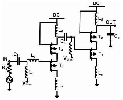
Figure 1. Designed LNA Circuit
High data rate implantable wireless systems come with many challenges, chief among them being low power operation and high path loss. LNAs designed for this application must include high gain, Low Noise Figure (NF) and better linearity at low power consumption within the required frequency. In this paper, the authors design is based on Impulse Response (IR) Ultra Wide-Band (UWB) operating at (3.1 – 5) GHz. They report the design and measurement of an LNA with 2.4dB NF, 17.3dB of gain and input intercept point of 2dBm consuming 4mW, which make it suitable for implantable radio applications. The process technology used here is 0.25μm CMOS Silicon on Sapphire (SOS) process.
The first stage of receiver front end has the dominant effect on the noise performance of the overall system. Compromises must be made as simultaneous optimal noise and gain much is typically not possible. Here, instead, noise figure is sought without degrading linearity. The desired goal for the LNA design was achieved using the cascade amplifier design topology. This topology has been more popular for narrow band, but modified for wideband applications with various input matching methods as discussed in [1] for current reused and [2] for CMOS LNA design optimization techniques.
According to [2], [4] source degeneration inductors are important for LNA performance improvement and area minimization. A source degeneration inductor has been introduced here to improve the linearity of the amplifier, a technique similar to the push-pull LNA in [2].
Impedance and noise matching over a wideband is the most challenging task to design a wideband low-noise amplifier which is crucial to a UWB system [3]. The inductive high-pass filter is designed as the input matching stage for a wideband characteristic. The input inductive high-pass network will filter out all frequencies lower than 3GHz. This network with the source degeneration inductor (Ls) and the intrinsic capacitances of transistor (T1) combine to achieve a wideband width matching to 50Ω as shown in Figure 1.
The circuit has been designed by selection of transistor operating points such that the amplifier gain does not degrade as much and IP3 is still maintained. A source degeneration inductor (Ls) was added to improve the amplifier linearity thereby reducing the amplifier gain, but subsequent stages were added to complement for the reduced gain. Lager values of Ls, improves the amplifier linearity but degrades gain and noise figure, so a careful selection was made to achieve low noise figure and a considerable gain. The complete circuit is shown in Figure 2.
Figure 1. Designed LNA Circuit
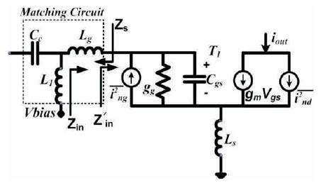
Figure 2. Equivalent Circuit for Input Matching Network
The implemented LNA designed, consists of two cascaded amplifier circuit, the first stage is optimized for noise performance and the second for linearity. The noise parameters of a cascade amplifier can be given by;
where, Gn is the equivalent noise conductance of the transistor, Rs is the source resistance, ωT is the cut-off frequency, γ is the coefficient of drain noise, δ is the coefficient of gate noise and c is the correlation term. It should be noted that, the noise parameter Zopt are for cascade amplifier with no degeneration as mentioned in [1], hence it is neglected in this design.
The source degeneration generates the real part at the input impedance. This became necessary, because there is no real part in ZOpt. Hence little value of Ls helps to reduce the discrepancy between the real parts of ZOpt. and Zin of the LNA. The imaginary part of Zin is changed by jω Ls, and this followed by the same change in ZOpt. as Opt shown below;
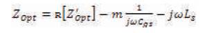
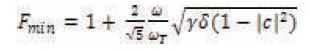
where, the constant m stands for the typical parameter of long channel MOSFETs, and is approximately equal to 0.6.with 0.25μm technology scaling, c is approximately 0.5 such that m is expected to be closer to 1.
Hence, the inductive source degeneration helps to bring ZOpt. point closer to the optimum source impedance point Z*in while causing no degradation in Fmin and Rn. This characteristic reveals the potential of common source with degeneration inductor.
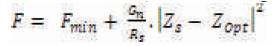
A Figure of Merit (FoM) suitable for evaluating the performance of wideband amplifiers can be defined as follows;
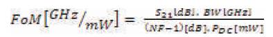
The circuit was well protected against Electrostatic Discharge (ESD); all signal pads and DC pads are ESD protected. Figures 3 & 4 shows the S-parameters of the designed common source LNA with source degeneration inductor, measured across (3 – 5) GHz frequency range. The values of S and S are less than -7.2dB, and -7.5dBm 11 22 respectively. The noise figure was also measured to be 2.3dB. The P1dB at 3.5GHz was measured to be -20dBm, and IIP3 is 2dBm. The power drawn from a 1.2V voltage source is 4mW. The FoM of the LNA was calculated to be 6.7GHz/mW. The state-of-the-art is shown in Table 1, comparing LNA design in 130nm CMOS technology with 0.25μm CMOS SOS.
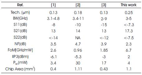
Table 1. LNA State-of-the-Art
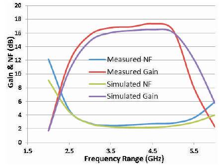
Figure 3. Measured LNA Gain and Noise Figure
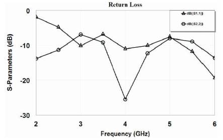
Figure 4. Measured Input and Output Return loss
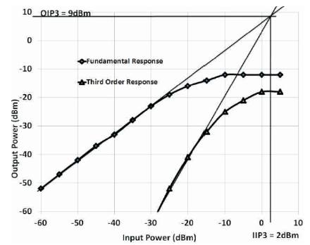
Figure 5. Measured IIP3 of Designed LNA
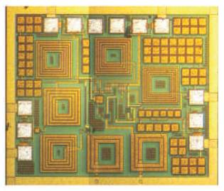
Figure 6. Designed LNA Micrograph
This project is partially funded by the David Skellern Electronics Research Grant and additional funding provided by a Macquarie University Concentration of Research Excellence grant.