Figure 1. Structure of QCA Geometry
Quantum-dot Cellular Automata (QCA) is promising solutions to design ultra-low power and very high speed digital circuits from among the recently emerging technologies alternate to Classic CMOS. Several researchers have demonstrated efficient QCA-based implementations for several binary and decimal arithmetic circuits, though significant improvements are still possible, exploitation of logic gates inherently available within the QCA technology is likely to provide better results. Signal Distribution Network (SDN) is one of the effective methods for the design of combinational and sequential circuits in quantum dot cellular automata. It overcomes the fabrication errors and thermal effects which occurred in wire crossings. The main objective is to increase the speed of digital circuits in QCA with the help of SDN. The main goal of this work is to reduce the hardware requirements of the digital logic circuits by using majority logic gate. The cell count and area can be reduced by logic synthesis. The main feature of SDN is it uses 4N-2 clock states for N number of inputs that is for the design of SDN and number of clock cycles required for the combinational circuit depends upon the number of stages. This paper describes the design of 2 to 4 line decoder, 4*1 Multiplexer 1*4 demultiplexer for QCA. Designed circuits are simulated by using QCA designer V2.0.3 software and calculated the delay of each circuit designed and the area occupied by the designed circuit.
The microelectronics industry has improved the integration, the power consumption, and the speed of integrated circuits during past several decades by means of reducing the feature size of transistors. But it seems that even by decreasing the transistor sizes, some problems such as power consumption cannot be ignored. Utilizing the QCA technology for implementing logic circuits is one of the approaches which in addition to decreasing the size of logic circuits and increasing the clock frequency of these circuits thus reduces the power consumption of these circuits. QCA, which was first introduced by Lent, Tougaw, Porod, and Bernstein, (1993) represents an emerging technology at the nanotechnology level. QCA cells have quantum dots, in which the position of electrons will determine the binary levels of 0 and 1. Quantum-dot Cellular Automata (QCA) is one of the emerging nano technologies that serve as alternative to CMOS technology with smaller area and low power consumption. Many designs of digital circuits, were proposed in QCA layout but not all are practically implementable due to random clocks in the design. There is a need for proper clocking scheme (Chandra, Suresh, & Ghosh, 2014).
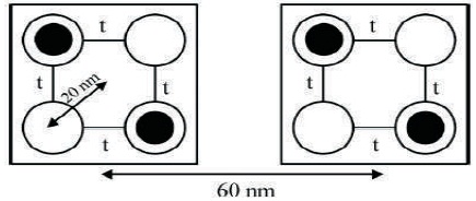
QCA design is developed by the ATIPS lab at the University of Calgary in Canada (Walus, Dimitrov, Jullien, & Miller, 2003). This software is used to simulate QCA circuits with coherence vector and bistable approximation engines. One of the main problems with this software and others is that they use the Landauer clocking and are unable to deal with multi types of clocking signals. It must be mentioned that the simulation of modules with large number of inputs and outputs, may take several hours or it may be impossible with this software. Ottavi, Schiano, Lombardi, and Tougaw, (2006) used Verilog to describe QCA devices, but he could not expand his library to include the dynamic behavior of QCA devices. Niemier (2003) introduced the QCA-LG that was a tool for the automatic layout generation of QCA combinational circuits. This tool generates the QCA circuit of an HDL input. QCA devices are designed by carefully selecting the placement of QCA cells and the timing with which their tunneling barriers are raised and lowered. As shown in Figure 1, a QCA cell is typically composed of four quantum dots located at the four corners of a square. Tunneling is allowed between adjacent dots, and the cell occupancy is controlled by a back plane voltage so that a total of two electrons occupy each four-site cell. The electrons in each cell coulombically repel each other, so the cell will typically exhibit one of two antipodal states, either pointing diagonally left (a binary 0) or diagonally right (a binary 1). Electrons in nearby cells will also interact with each other coulombically, causing adjacent cells along the same linear axis to align in the same direction.
Figure 1 QCA geometry used in this paper. Each cell is composed of four quantum dots, with two electrons sharing each four-site cell. Sites are 20 nm from the center of the cell, and adjacent cells are 60 nm apart. Tunneling is allowed between adjacent sites within the cell, and electron repulsion leads to a bistable alignment into one of two states, which are used to encode a binary 0 and a binary 1.
Figure 1. Structure of QCA Geometry
By carefully arranging the location of QCA cells, it is possible to create a majority logic gate, which is capable of functioning as either an AND or an OR gate (Tougaw & Lent, 1994). Combining these gates with the QCA cell configuration of an inverter, any combinational logical device can be constructed from QCA cells (Lent & Tougaw, 1997). The dynamics of the array can be solved directly, retaining the full many-electron degrees of freedom only for small array sizes. For larger arrays, we develop several approximate techniques for reducing the size of the basis set required (Tougaw & Lent, 1996). Although the foundations of QCA have been firmly established, there are several areas of QCA research that remain very active. One active area of QCA research is seeking to understand the behavior of the devices in the presence of thermal effects and fabrication imperfections (Orlov et al., 2000; Anduwan et al., 2010; Khatun, Barclay, Sturzu, & Tougaw, 2006; Khatun, Barclay, Sturzu, & Tougaw, 2005; Khatun, Padgett, Anduwan, Sturzu, & Tougaw, 2013; LaRue, Tougaw, & Will, 2003; Pasky, Henry, & Tougaw, 2000). Studying the robustness of QCA devices in the presence of these effects has illustrated the importance of the excitation energy, which is the difference between the device's ground-state energy and the energy of its first excited state. The larger this energy, the more robust and reliable the behavior of the device (Anduwan et al., 2010). Canonical ensemble, a Hubbard-type Hamiltonian and the inter-cellular Hartree approximation were used, and a statistical model has been introduced to simulate defects in the QCA devices (Khatun et al., 2006).
These QCA cells are arranged in a wired fashion (2- dimensional) or three dimensional manner for transfer of information and for performing different operations. This arrangement can be done by using wire crossings . Due to neighbourhood interactions in coplanar wire crossing, the excitation energy is reduced which will lead to fabrication errors. One method to overcome the drawbacks of the wire crossings is the use of second near neighbour interactions in wire crossings. But the disadvantage of this method is, it is highly susceptible to thermal effects. Other solution is the use of revolving door.
It depends on ''RD'' cell to which the signalling is given so that it first passes the horizontal signals and the control is then hand over to pass vertical signals. This revolving door technique is suitable for small circuits. If the size of the circuit increases, the complexity of using revolving door increases. This technique requires three additional clock signals: one is RD cell, one each to receive and store the signals horizontally and then vertically. These are indicated by “SD1” and “SD2”, which increases the complexity of the circuit.
In order to overcome the drawbacks mentioned above, Signal Distribution Network is used with 4 distinct clocks as shown in the Figure 2. The use of additional clock signals in revolving door technique can be rectified by using signal distribution network which uses 4 distinct clock signals.
Each clock cycle consists of 4 states or regions as shown in Figure 2. The states are switch, hold, release, are relax. In switch phase, the tunnelling barriers are raised between the dots and a particular state is attained and is hold during hold state and acts as an input to the neighbouring cells. In release phase, the tunnelling barriers are lowered. In relax phase, there is no barrier between two dots and the cell can be in any state. When an input is given to the cell, the cell is in switch state and after it enters into hold state which acts an input to the next state. By the change of states, the information is transferred from one cell to the other cell and basic logic gates like AND, OR, and NOT gates can be implemented. Remaining gates can be derived from the basic logic gates.
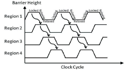
Figure 2. Clock Direction in Signal Distribution Network
A Quantum Cellular Automaton (QCA) is an abstract model of quantum computation, devised in analogy to conventional models of cellular automata introduced by von Neumann. The same name may also refer to quantum dot cellular automata, which are a proposed physical implementation of "classical" cellular automata by exploiting mechanical phenomena. QCA have attracted a lot of attention as a result of its extremely small feature size (at the molecular or even atomic scale) and its ultra-low power consumption, making it one candidate for replacing CMOS technology. In the context of models of computation or of physical systems, quantum cellular automaton refers to the merger of elements of both (1) the study of cellular automata in conventional computer science and (2) the study of quantum information processing. In particular, the following are features of models of quantum cellular automata:
Another feature that is often considered important for a model of quantum cellular automata is that it should be universal for quantum computation (i.e. it can efficiently simulate quantum turing machines, some arbitrary quantum circuit or simply all other quantum cellular automata).
The computation is considered to come about by parallel operation of multiple computing devices or cells. The cells are usually taken to be identical, finite dimensional quantum systems (e.g. each cell is a qubit).
QCA cell consists of four quantum dots arranged at the corners of the square as shown in the Figure 3. The circles which are filled indicates the presence of an excess electron. The two representations of quantum cell: one in which the dots are diagonally left represents classical bit '0'and the other in which the dots are diagonally left represents classical bit ‘1' shown in Figure 3.
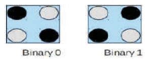
Figure 3. Representation of QCA Cell
The Signal Distribution Network is one of the solution to overcome the draw backs of wire crossing. SDN is designed with in the same area which was used for wire crossings. SDN directs the signals to the logic gates (combinational circuit) and functions similar to the wire crossings. The block diagram for SDN is shown in the Figure 4.
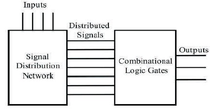
Figure 4. Separation of the function into signal distribution and combinational logic
Figure 4 represents separation of the function into signal distribution and combinational logic. This separation allows for the use of an optimized, highly regular signal distribution network, followed by a similarly optimized combinational logic block without the need for interspersed wire crossings. The number of inputs, distributed signals, and outputs are entirely arbitrary.
When the signal distribution network has done the work, signals are distributed to the combinational circuit and the crossings are eliminated in this region. The design of SDN depends upon the delay of the circuit which is 4n-2 clock cycles, where n is number of inputs. For example, if the number of inputs are 3, then the number of clock states required for SDN are 10. As the number of inputs increases, the number of clock cycles increases. This process of distributing signals to the combinational circuits will decrease the delay compared with the wire crossings.
The crossings are eliminated in SDN which increases the excitation energy so that the fabrication errors can be minimised. By the use of SDN, thermal effects can be reduced. The robustness of the device increases as the excitation energy increases in the SDN.
Furthermore, the area of the SDN is decreased by an approach named 'Scalable Signal Distribution Network' (SSDN). In this the area of the SDN can be reduced by using a single distribution line instead of using the number of distribution lines which equals to the number of inputs. The delay of the QCA circuit using SDN and SSDN are same. The circuits are designed and simulated by using QCA Designer tool and verified outputs for all combinations of inputs.
3.1 2 to 4 Decoder using SDN
A 2 to 4 decoder consists of 2 inputs and 4 outputs and it is an AND logic. To design the decoder circuit using SDN in QCA, instead of 2-input AND gate, a 3-input majority gate is used. It requires 4n-2 i.e.,10 clock states for SDN and 2 clock states for combinational circuit to work. Therefore a total of 12 clock states (3 clock cycles) are required.
In the Figures 5 and 6, inputs are A, B, C and y0,y1,y2,y3 are outputs. To act as an AND gate the input to the C is bit '0'. The delay is indicated by the colour inversion at the output. After 12 clock states (3 clock cycles) output is observed.
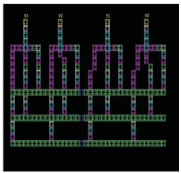
Figure 5. Design of 2 to 4 Decoder using SDN
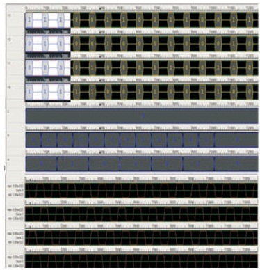
Figure 6. Simulation Results of 2 to 4 Decoder
3.2 1*4 Demultiplexer using SDN
A 1*4 demultiplexer has 1 input ,2 selection lines and 4 outputs and it is an AND logic. To design the demultiplexer, a 3 input majority gate is used instead of 2 input and gate. It requires 4n-2 i.e., 14 clock states for SDN and 2 clock states for combinational network. Therefore a total of 16 clock states (4 clock cycles) are required.
In the Figures 7 and 8, the inputs A, B, C and the outputs are y0,y1,y2,y3. To indicate the delay (4 clock cycles) at the output the colour of the output waveform is inverted.
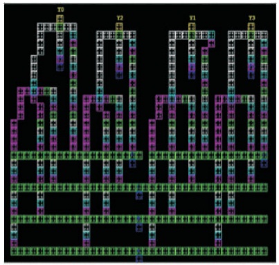
Figure 7. Design of 1*4 Demux using SDN for QCA
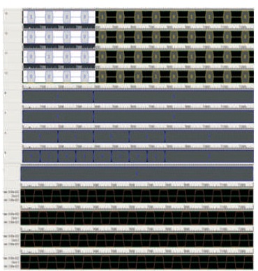
Figure 8. Simulation Results of 1*4 Demultiplexer
A 4*1 multiplexer has 4 inputs, 1 output and 2 selection lines and it is an AND-OR logic. 3-input majority gate can be used instead of 2-input AND, 2-input OR gates. It requires 4n-2 i.e., 26 clock states and an extra 2 clock states for the combinational circuit to work. Thus a total of 28 clock states (7 clock cycles) is required to get desired output.
In the Figures 9 and 10, A, B, C, D3, D2, D1, D0 are the inputs and y3, y2, y1, y0 are the outputs of AND gates (implemented majority gate as AND gate). To indicate the delay (7 clock cycles) at the output, colour of the output waveform is inverted.
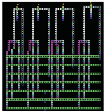
Figure 9. Design of 4*1 Mux using SDN
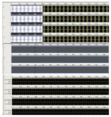
Figure 10. Simulation Results of 4*1 Multiplexer
From the Table 1 comparison, it is observed that as the number of inputs increases the area of the circuit increases and delay of the circuit increases.
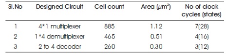
Table 1. Comparsion of area and delay of the designed circuits
SDN allows 4n-2 clock states for n number of inputs. SDN depends on the strongest interaction between cells that lies on the same line. Therefore, there is no decrease in the excitation energy compared with coplanar wire crossing. There is a vast scope in developing both combinational and sequential circuits using Signal Distribution Network (SDN) and also development in the design of circuits using Scalable Signal Distribution Network (SSDN). The area comparisons are shown by considering three logics. To make the work easier the design of the SDN can be extended to code converters of codes like BCD, Excess-3. Memory cells of higher bit capacity can be effectively designed. Highly regular clocking schemes can be enhanced to ripple clock scheme which results in an hazard free circuit mainly for sequential circuits. QCA is in the tender stage of research and development. QCA can be developed further by minimising the area and power factor. One of the greatest challenge is to design a simulation tool that supports the parameters like synchronisation. Further, this concept is enhanced by using PTL logic for further reduction of power consumption. As PTL (Pass Transistor Logic) is more usefull to reduce the number of transistors required to design any logic, while compare with CMOS.