(1)
In this paper, the concentration of halo implant and threshold implant has been varied to estimate the sub-threshold leakage current and substrate current of the MOSFET. A lightly doped NMOS has been designed having channel length of 40 nm in Athena and simulated in Atlas of Silvaco TCAD tool. After simulation results, it has been observed that as the threshold implant and halo implant concentrations are increased, there is a decrease in both off-state sub-threshold leakage and substrate current as required for an ideal MOSFET. Other parameters like ON current, DIBL, and threshold voltage have also been estimated.
Device modelling and simulation can be used to estimate the electrical characteristics of the any device. Scaling down MOSFETs leads to improved packaging density, speed, and power dissipation. Before performing actual fabrication process which is very costlier and time consuming, virtual fabrication can be done using any Technology Computer Aided Design (TCAD) tool to calculate design and fabrication parameters for decreasing design costs, enlightening device design yield and attaining better device and technology designs (Berkley Predective Technology model). Theoretically, the threshold voltage is simply the applied gate-to-source voltage needed to turn on a MOS device. The threshold voltage for a long channel device can be approximated by solving the one-dimensional Poisson's equation:
For an n-channel device,
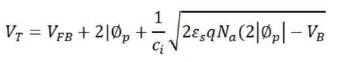
Here VFB is the flat-band voltage, ci is the insulator capacitance, q is charge carrier density, εs is the dielectric permittivity of the semiconductor, and VB is the bulk bias (Dwivedi et al., 2015).
While,
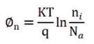
Na is the acceptor dopant concentrations in the substrate, k is Boltzmann constant, T is the absolute temperature, and ni is the intrinsic electron density. Note that the threshold voltage is strongly dependent on doping concentration (ITRS, 2003).
Halo implant concentration and threshold implant concentration are two important parameters to adjust the vital parameters of the MOSFET. During fabrication process, by changing the concentration of these two parameters, off current, threshold voltage, sub-threshold current, and DIBL can be adjusted to improve the performance of the device. A 45 nm NMOS device has been designed and virtually fabricated in Athena and Atlas of Silvaco TCAD tool.
Atlas is a 2D and 3D device simulator that performs DC, AC, and transient analysis for silicon, binary, ternary, and quaternary material-based devices. Atlas enables the characterization and optimization of semiconductor devices for a wide range of technologies.
The objective of the paper is to analyse the effect of halo implant and threshold voltage implant on the electrical characteristics of NMOS device.
The structure of 45 nm NMOS is shown in Figure 1.
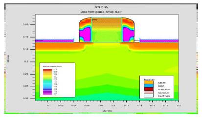
Figure 1. Structure of 45 nm NMOS
The NMOS structure has been designed using specifications given in Table 1. The physical Gate length is 40 nm and substrate is lightly doped having doping concentration of 5 e15cm-3 . Initially, the device is designed using threshold implant of concentration 5 e12cm-3 and halo implant of concentration 5 e13cm-3 and further it is varied to analyse the effects of concentration on leakage current, ON current, OFF current, DIBL, threshold voltage, and substrate current (ITRS, 2007).
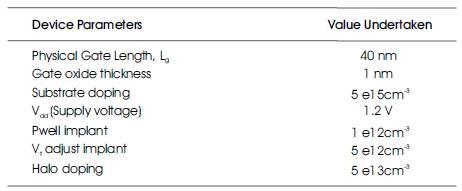
Table 1. Specifications of 45 nm NMOS
After design and simulation of NMOS device, the drain current versus gate voltage characteristics have been plotted as shown in Figures 2 and 3.

Figure 2. ID versus VDS Plot in Linear Scale for different Gate Voltages
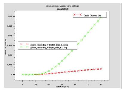
Figure 3. ID versus VGS Plot in Linear Scale for different Drain Voltages
Present day MOS process invariably use ion implantation into the channel region, a step often called the threshold adjusts implant that alters the doping profile near the surface of silicon substrate. The optimized threshold voltage can be achieved by changing dose and energy of the threshold implant. The threshold voltage is by no means a constant quantity but varies with the back bias (Zabeli et al., 2008; Sachdeva et al., 2017a). The structure with different threshold implants are shown in Figure 4 and drain current characteristics are shown in Figure 5.

Figure 4. NMOS Structure with different Threshold Implants
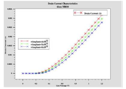
Figure 5. ID versus VGS Plot in Linear Scale for different Threshold Implants
As the concentration of threshold adjust implant increases, the threshold voltage increases and the drain current starts to decrease as shown in Figure 6. This implant is basically to adjust threshold voltage.
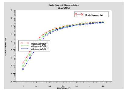
Figure 6. ID versus VGS Plot in Log Scale for different Threshold Implants
As the threshold voltage implant concentration increases, the substrate current of the device decreases as required for an ideal device is shown in Figures 7 and 8. Table 2 shows the estimation of various parameters of MOSFET with the variation of threshold implant. These parameters are extracted after the simulation performed in ATLAS simulator. It shows that as the concentration increases, ON current decreases, OFF state leakage current decreases, ON/OFF ratio increases, sub-threshold slope has been improved, substrate current and DIBL decreases which plays an important role for leakage current of the device (Sachdeva et al., 2017b; Ortiz-Conde, 2013).
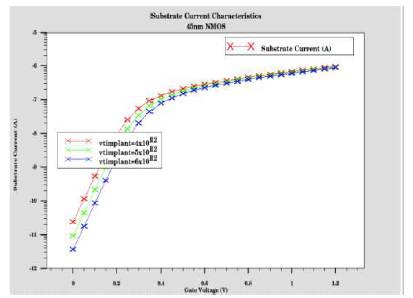
Figure 7. ISUB versus VGS Plot in Log Scale for different Threshold Implants
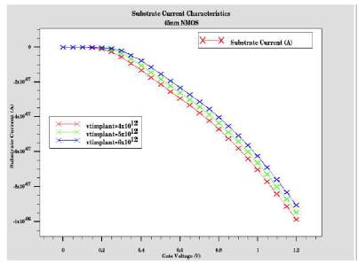
Figure 8. ISUB versus VGS Plot in Linear for different Threshold Implants
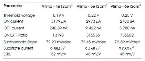
Table 2. Extracted Parameters for different threshold Implants
Figure 9 shows the decrease of OFF state leakage current in subthreshold region at different threshold implant concentrations.
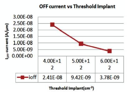
Figure 9. OFF Current at different Threshold Implants
Figure 10 shows the decrease in substrate current as the threshold adjusts implant increases.

Figure 10. Substrate Current at different Threshold Implants
Figure 11 shows that as the concentration of threshold voltage implant increases, the Drain Current Barrier Lowering (DIBL) decreases. The threshold voltage is a measure of the strength of the barrier against carrier injection from the source to the channel. As the voltage between the source and drain increases, the depletion region under the drain will lower the potential barrier from the source to the channel junction (Osthaug et al., 2004; Silvaco International, 1995).
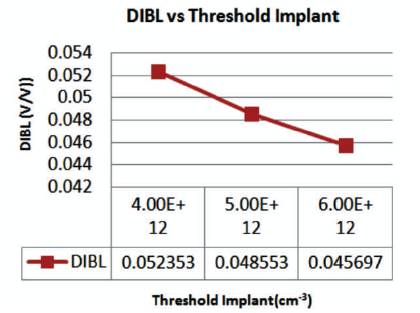
Figure 11. DIBL at different Threshold Implants
The variation of concentration of halo/pocket implants is another technique that can improve short channel effects and thereby control the threshold voltage roll-off. Halo doping or non-uniform channel profile in a lateral direction is another way to regulate the dependence of threshold voltage on channel length. For n-channel MOSFETs, very highly p-doped regions are introduced near the two ends of the channel which reduces the charge-sharing effects from the source and drain. Charge sharing effects are reduced which further reduces the threshold voltage of the device. Thus, threshold voltage becomes more nearly independent on channel length. Hence, the OFF state leakage current becomes less sensitive to channel length variation (Kang and Leblebici, 2003).
Figure 12 shows the structure with different pocket implant concentrations.
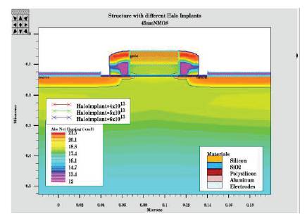
Figure 12. NMOS Structure with different Halo Implants
Figure 13 represents the plot of ID versus VGS in linear Scale for different Halo implants.
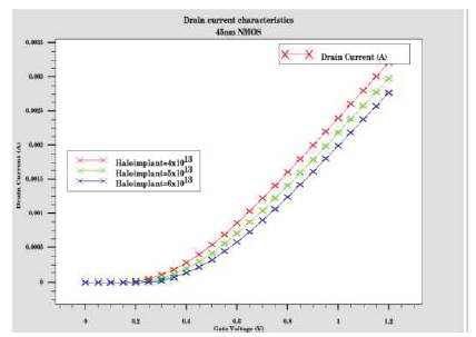
Figure 13. ID versus VGS Plot in Linear Scale for different Halo Implants
Figure 14 shows the variation of drain current with gate voltage at different drain voltages in linear and log scale. As the concentration of halo implant increases, there is a increase in threshold voltage and decrease in ON current of the device. This implant is basically for reducing the OFF current neglecting the ON current of the device.
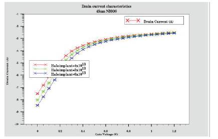
Figure 14. . ID versus VGS Plot in Log Scale for different Halo Implants
Figures 15 and 16 represent the decrease of substrate current with the increase of halo implant concentration. Table 3 shows the variation of various parameters with the variation in halo/pocket implant concentration. As the halo implant concentration increases, threshold voltage increases, ON current decreases, OFF state leakage current decreases, ON/OFF ratio increases, sub-threshold slope has been improved, substrate current and DIBL decreases which contributes in short channel effects.
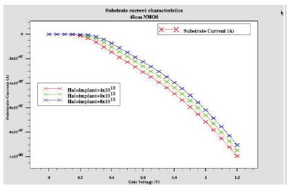
Figure 15. ISUB versus VGS Plot in linear for different Halo Implants
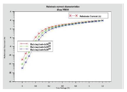
Figure 16. ISUB versus VGS Plot in Log Scale for different Halo Implants
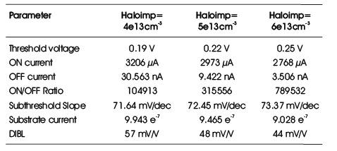
Table 3. Extracted Parameters for different Halo Implants
Figure 17 shows the decrease of OFF current with the increase in halo implant concentration.

Figure 17. OFF Current at different Halo Implants
Figure 18 shows the decrease of substrate current with the increase in halo implant concentration.
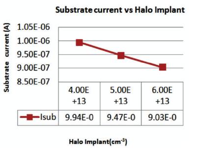
Figure 18. Substrate Current at different Halo Implants
Figure 19 shows the decrease of DIBL with the increase in halo implant concentration. When the barrier between the source and the channel is decreased, there will be more added electrons into the channel region causing excess injection of charge carries into the channel region that gives an increased OFF state leakage current. This results in lowering of the threshold voltage and the gate has reduced control over the channel current. This is called DIBL.
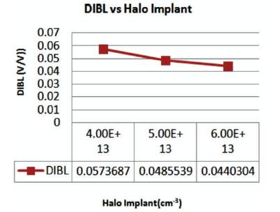
Figure 19. DIBL at different Halo Implants
Both the threshold implant and halo implant parameters are varied during fabrication, to get optimized OFF state leakage current of 9.422 nA, threshold voltage of 0.22 V, substrate current of 72.45 mV/dec, and DIBL of 48 mV/V at 1nm gate oxide thickness. The best value of threshold implant seems to be 5e12cm-3 and halo implant is 5e13cm-3 . This also improves ON/IOFF ratio that make the device to have higher current drive and lower leakage current at OFF state. Results presented in this paper will be useful in design and optimization of MOSFET electrical characteristics.