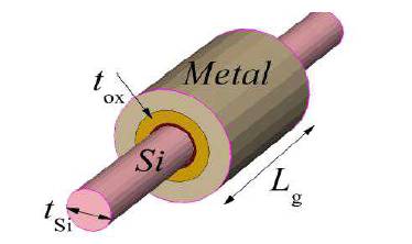
Figure 1. Schematic Structure of Cylindrical Gate All Around (GAA) MOSFET
This paper investigates the effect of the work function on 45 nm gate length, cylindrical gate all around MOSFET and evaluates the short channel performance of the device using gate electrode work function analysis. In this work, the sensitivity of gate work function (φM) on various performance metrics like threshold voltage (Vt ), On current (ION ), subthreshold leakage current (IOFF ), On-Off current ratio (ION /IOFF ), Subthreshold slope and DIBL (Drain Induced Barrier Lowering) of cylindrical GAA are systematically evaluated and analysed. The SCE (Short Channel Effects) can sensibly be controlled and improved by proper adjustment of the metal gate work-function. In the present study, all the device performances are investigated through ATLAS device simulator from Silvaco.
The continuous downscaling of MOS device has remained imperative need for the aggressive scaling in package density and performance, leading to efficient chip functionality at higher speeds. However, the scaling of Metal-oxide-semiconductor Field Effect Transistor (MOSFET) will degrade the gate control over the channel due to close proximity between source and drain (Chaudhry and Kumar, 2004; Young, 1989). Cylindrical Gate All Around (GAA) MOSFET is a major invention and most promising candidate to replace conventional MOSFET, fit into next generation (Zhang et al., 2010; Chiang and Liou, 2013; Pratap et al., 2014). As the threshold voltage degrades, the cylindrical gate all around MOSFET also suffers from short channel effects and subthreshold leakage current (Bangsaruntip et al., 2010; Chiang, 2011). A metal gate technology can prevail over this limitation by providing the desirable gate work function (Mustafa et al., 2013). We can also set the desirable threshold voltage by channel doping, but it decreases the device performance due to the dopant fluctuations, carrier mobility degradation, and large subthreshold slope (Zhou et al., 1999). As we increase channel doping, it increases band to band tunneling between body and drain and hence the performance of gate all around MOSFET degrades (Chang et al., 2000). It draws attention towards gate work function as an alternative solution (Siliconix, 2010). In order to minimize the leakage current the metal gate is used for submicron technology (Ana, 2011). Metal gate electrode desires to regulate threshold voltage to a preferred value in order to decrease short channel effects (Tsui and Huang, 2003). In this study the effect of gate electrode work function on various electrical characteristics like threshold voltage (Vt ), On current (ION ), subthreshold leakage current (IOFF ), On-Off current ratio (ION /IOFF ) and DIBL (Drain Induced Barrier Lowering) are explored using Atlas Device Simulator. Atlas is a 2D and 3D device simulator that performs DC, AC, and transient analysis for silicon, binary, ternary, and quaternary material-based devices. Atlas enables the characterization and optimization of semiconductor devices for a wide range of technological. properties for the commonly used semiconductor materials in use today.
The schematic diagram of the cylindrical gate all around (CGAA) MOSFET structures used for simulation is shown in Figure 1. This structure is implemented using Atlas Silvaco tool. The radial directions are assumed to be along radius and lateral direction along z-axis of the cylinder as shown in Figure 1.
Figure 1. Schematic Structure of Cylindrical Gate All Around (GAA) MOSFET
The details of device physical parameters used in the structure are shown in Table 1. SOI (Silicon On Insulator) substrate in cylindrical gate all around (GAA) MOSFETs have n-type channels. The Length of the gate (Lg ) is 45 nm and radius of 5 nm. Gate oxide thickness of SiO2 (tox ) is 1 nm.
Table 1. Device Dimensions and Dopings
The source/drain extension doping profile was set as Gaussian with the peak concentration of 1.0 x 1020 cm-3 . The authors investigated threshold voltage (Vt ), On Current (ION ), Off Current (IOFF ), On-Off current (ION /IOFF ) ratio and DIBL (Drain Induced Barrier Lowering) variation for the gate work function ranging from 4.4 to 4.6 eV in the present simulation study.
Figure 2 shows the drain current Ids versus gate voltage Vgs characteristics of cylindrical gate all around MOSFET for different values of gate work function. The metal gate work function has been varied from 4.4 eV to 4.6 eV. The results show that the subthreshold behaviour of device advances, as the metal gate work function is increased to higher values. It is because of the fact that as the metal gate work function increases, the corresponding threshold voltage also increases, which in turn decreases the off-state leakage current and results in the enhancement in the device performance. This is very desirable characteristics of the device for various applications.
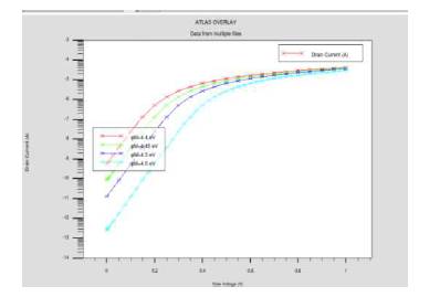
Figure 2. Ids versus Vgs Curve for Different Work Function
Since the metal gate work function can be accustomed to meet a given threshold voltage requirement, the choice of the metal gate material will depend upon the metal which offers the suitable work function for preferred threshold voltage. Vt is defined as,
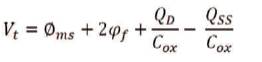
where Qss represents the charge in gate dielectric, Cox is the gate oxide capacitance, φms is the work function difference between semiconductor and gate electrode, φf is the difference between the semiconductor Fermi level Ef and the intrinsic semiconductor Fermi level EFi . They investigated the threshold voltage (Vt ) variation for the gate work function ranging from 4.4 to 4.6 eV in the present simulation study. It has been analyzed that by increasing the gate work function of cylindrical gate all around MOSFET, the corresponding threshold voltage increases to a desired value as shown in Figure 3. The results as shown in this figure have been obtained for a device having Lg = 45 nm, R = 5 nm, tox = 1 nm.
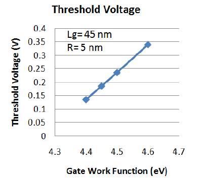
Figure 3. Threshold Voltage Variation with Different Gate Work Function
The device on-current behavior as a function of gate work function has been illustrated in Figure 4. It is clear that device on-current is suffered as threshold voltage increased with increase in metal gate work function of cylindrical gate all around MOSFET structure.
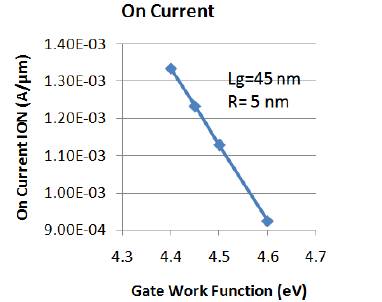
Figure 4. On-Current Behaviour with Variation of Gate Work Function
The device off-current behavior as a function of gate work function has been illustrated in Figure 5. It is clear that device off-current also decreases as increase in metal gate work function of cylindrical gate all around MOSFET structure.
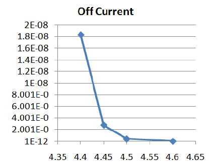
Figure 5. Leakage Current Analysis for Different Gate Work Function
The device ION /IOFF current ratio behavior as a function of gate work function has been illustrated in Figure 6. It is clear that device ION /IOFF current ratio increases as increase in gate work function of cylindrical gate all around MOSFET structure.
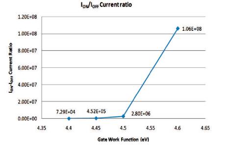
Figure 6. ION /IOFF Current Ratio Variation with Gate Work Function
The Drain Induced Barrier Lowering (DIBL) effect is defined as the lateral shift of the transfer curves in the subthreshold regime when the drain voltage varies from 0.05 V to 1 V.
The DIBL behaviour as a function of gate work function has been illustrated in Figure 7.
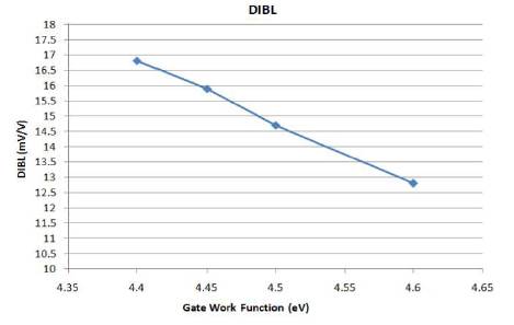
Figure 7. DIBL Variation with Gate Work Function
The result of simulation were summarised in Table 2.
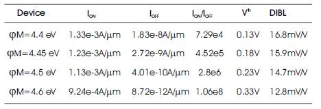
Table 2. Simulated Value of Cylindrical Gate all Around MOSFET's Electrical Characteristics for different Values of Gate Work Function of the Structure
It has been analysed that device has higher driving current and leakage current for work function 4.4 eV as matched to work function 4.5 eV and 4.6 eV. But the ratio of ION /IOFF current increases by increasing the work function ranging from 4.4 eV to 4.6 eV. It is also observed that Cylindrical GAA MOSFET having work function 4.6 eV has higher threshold voltage and lower DIBL effect. So in this way we can advance the device performance by reducing the leakage current with variation of work function in sub-threshold regime.