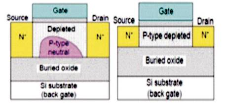
Figure 1. Partially Depleted and Fully Depleted SOI MOSFET
Currently, the expansion of VLSI industry is primarily focussed on the way to the efficiency of semiconductor devices which in turn is extremely dependent on the advancement in the CMOS technology. As the scaling down of device dimensions are being aggressive, gate tunnelling effect, p-n junction leakage current increases, and sub-threshold slope increases. More precise and novel device structures are required to be developed for overcoming the above mentioned problems. These needs have led to the development of alternative technology. So SOI technology has been invented with a buried oxide layer in the silicon substrate. Due to the isolation created by this buried oxide in the substrate, various short channel effects have been reduced. This paper presents an electrical comparison between a 45 nm n-channel Metal Oxide Semiconductor Field Effect Transistor (NMOSFET) and 45 nm Silicon On Insulator (SOI) MOSFET simulated using SILVACO ATLAS simulator. The fabrication of both the devices have been carried out in SILVACO TCAD software and estimation of threshold voltage, drain current, and sub-threshold slope has been done. Drain current versus gate voltage and drain current versus drain voltage curves have been plotted and compared. By comparing the characteristics of the bulk and SOI MOSFET, the SOI MOSFET has been found to be better than the bulk NMOSFET.
In a conventional bulk NMOSFET, the active elements are located in a thin surface layer approximately less than 0.5 μm of thickness which are isolated from the silicon body with a depletion layer of a p-n junction. The leakage current of this p-n junction exponentially increases with temperature, and is responsible for several serious reliability problems. At high temperature, excessive leakage current and high power dissipation limits the operation of microcircuits parasitic n-p-n and p-n-p transistors formed in neighbouring insulating tubs can cause latch-up failures and significantly degrade circuit performance. The objective of this paper is to simulate a bulk and a SOI MOSFET and study the electrical characteristics using SILVACO TCAD Tool. In the silicon-oninsulator (SOI) MOSFET, an insulator layer called buried oxide is established between the silicon layer and substrate of the semiconductor. It decreases the parasitic device capacitance. The silicon dioxide (SiO2 ) is widely used as insulator layer. There are many benefits of SOI MOSFETs over conventional MOSFETs as follows:
There are two types of SOI MOSFETs:
In the PD-SOI, the channel region between source and drain is partially depleted while the channel is completely depleted in case of FD-SOI. FD-SOI is preferred because of its thin size, low leakage currents, and enhanced power consumption characteristics. The partially depleted SOI and Fully depleted SOI have been shown in Figure1 below.
Figure 1. Partially Depleted and Fully Depleted SOI MOSFET
The objective of the study was to analyse the bulk MOSFET and SOI on the basis of various parameters, i.e subthreshold slope, drain current, and threshold voltage [8].
Process simulation involves the modelling of physical processes with the aim of studying their impact on the external environment and the objects they are applied to. In this paper, the authors have analysed MOSFETs in 45 nm technology, fabricated using SILVACO TCAD tool in which ATHENA is a modular program that allows for the simulation of a wide range of semiconductor fabrication processes: epitaxial growth, thermal oxidation, thermal diffusion and ion implantation, photolithography, etching, deposition dielectrics films, metallization and many others and combines these simulations into a more complete package. While on the other hand, SILVACO TCAD tool also provides with a physically-based device simulation program ATLAS which is responsible for predicting the electrical characteristics that are associated with specified physical structures and bias conditions of the fabricated device [1]. By applying a set of differential equations, derived from Maxwell's laws, the carriers are transported through structure, thus obtaining the characteristic accordingly. The final device structure is visualized on TONY PLOT module which includes animation features that permit viewing a sequence of plots in a manner showing solutions as a function of some parameter.
Figure 2 shows the flow of data in SILVACO TCAD tool which refers to Technology Computer-Aided Design. This means that computer aided simulator is used to evolve and optimize semiconductor processing technologies and devices. As TCAD simulations solve fundamental, physical partial differential equations, such as Poisson, Diffusion, and Transport equations in a semiconductor device. This physical approach gives computer aided design simulation, a predictive perfection. It is used to produce small layout test structures and then fabricate these structures using initial guess values for unknown process parameters [2]. Electrical simulation is then performed to determine if the device meets the device fabrication requirement. If not, the cycle is repeated with new sets of estimated process parameters. Usually, this whole cycle is used to repeat many times in order to obtain the desired results.
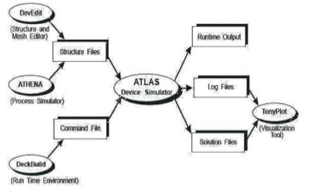
Figure 2. Flow of Data in SILVACO TCAD Tool
The threshold voltage expression in case of a MOSFET device structure can be expressed as,
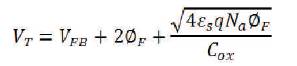
where VFB represents the flat band voltage, COK is the gate capacitance, ΦF is the bulk potential.
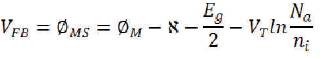
ΦMS represents metal-semiconductor work-function difference between the gate electrode and the semconductor, χ is the electron affinity,
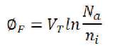
where NA is acceptor concentration which is 6e16 atoms/cm3 and niis intrinsic carrier concentration which is 1.45e10 atoms/cm3 . For 45 nm device, VFB comes out to be -0.6761,ΦF is 0.39 and thus the theoretical value of threshold voltage for this 45 nm device comes out to be 0.1 V, which is approximately equal to the simulated value [3, 4].
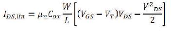
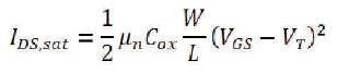
The Drain current of NMOS is given by the equation below that drain current is zero in cutoff region.

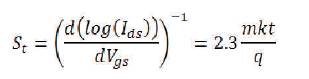
A plot of logarithmic drain current versus gate voltage is plotted. Its slope is the sub-threshold slope is given by:
The final structure of a bulk NMOS transistor and a SOI NMOS transistor is designed using Atlas after going through a group of process simulation products. The performance of bulk and SOI MOSFET has been compared depending upon various parameters.
In Figure 3, MOSFET is having substrate of n type semiconductor with p-type impurity having concentration of 6e16 atoms/cm3 . Source and Drain of NMOS transistor has n-type impurity concentration of 6e21 atoms/cm3 . The thickness of gate oxide is 2 nm. The threshold voltage achieved with the device is 0.19 V. ID -VGS characteristic for VDS =0.1 volt is obtained through ATLAS simulator [6].
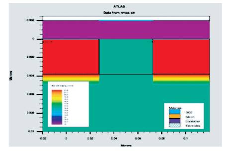
Figure 3. Structure of 45 nm Bulk NMOSFET
The log ID –VGS characteristics of 45 nm NMOS is shown in Figure 4.
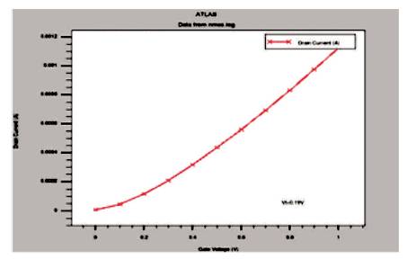
Figure 4. ID -VGS Characteristic of 45 nm NMOS
From the graph shown in Figure 5, the subthreshold slope obtained is 0.132 V/decade. The ID -VD curves for 45 nm NMOS is given in Figure 6. Three curves are plotted for 0.1 V, 0.5 V, and 1.2 V Drain voltages [7].
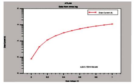
Figure 5. Log ID -VD Characteristic of 45 nm NMOS
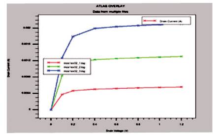
Figure 6. ID -VD Characteristic of 45 nm NMOS
SOI MOSFET is having a substrate of n type semiconductor with p-type impurity having concentration of 6e16. Source and Drain of NMOS transistor has n-type impurity concentration of 6e21 atoms/cm3 . The thickness of gate oxide is 2 nm [5]. The threshold voltage achieved with the device is 0.16 V. ID -VGS characteristic for VDS =0.1 volt is obtained through ATLAS simulator. SOI MOSFET is shown in Figure 7.
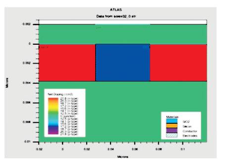
Figure 7. Structure of 45 nm SOI NOSFET
Figure 8 shows the linear ID –VGS characteristics for 45 nm SOI.
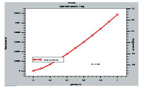
Figure 8. ID -VGS Characteristic of 45 nm SOI
The log plot ID –VGS characteristics for 45 nm SOI is given in Figure 9. This graph is used to calculate the value of sub threshold slope. From the graph, the sub threshold slope obtained is 0.122 V/decade. The ID -VD curves for 45 nm SOI NMOS is given in Figure 10. Three curves are plotted for 0.1 V, 0.5 V, and 1.2 V Drain voltages.
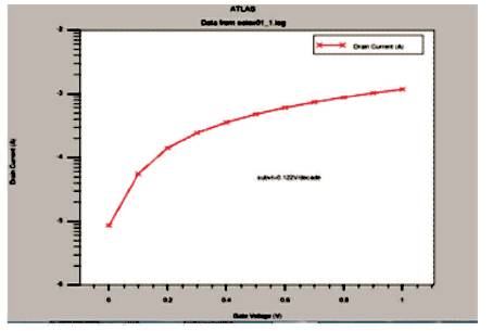
Figure 9. Log ID -VD Characteristic of 45 nm SOI
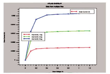
Figure 10. ID -VD Characteristic of 45 nm NMOS
Table 1 shows the comparison of bulk and SOI MOSFETs, which shows the reduced sub-threshold slope and threshold voltage [9].
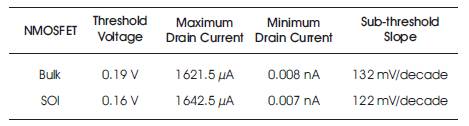
Table 1. Comparison of Bulk and SOI MOSFETs
This paper evaluates the electrical characteristics and performance comparison between bulk n-MOSFET and SOI n-MOSFET using SILVACO T-CAD Simulator at 45 nm technology. Electrical characteristics, such as threshold voltage, sub-threshold slope, and drain current are extracted using Silvaco ATLAS. It is concluded that the introduction of an oxide layer below the channel in the NMOSFET device improves the performance parameters due to the isolation of the channel from the body. The threshold voltage gets reduced, and the drain current increases in the SOI MOSFET as compared to the bulk MOSFET.
The authors would like to take this opportunity to express their gratitude to Faculty of Electronics and Communication Engineering, YMCA University Faridabad and the laboratory staff for their support, guidance and for the facilities used to make this study a successful one.