Figure 1. Circuits Explaining Adiabatic Switching
Fundamental and the core of all the Digital Signal Processors (DSPs) are its multipliers and speed of the DSPs is mainly determined by the speed of its multipliers. Multiplication is the most fundamental operation with intensive arithmetic computations. Now a days, embedded systems are used for wide range of such applications. The power consumption, performance, and demanding security are the main issues in designing systems. To achieve this, authors combined the sub-threshold operation and charge recovery techniques. Using the technique, lower power consumption, ability of operating at higher frequencies, and more security than the existing logic circuits are achieved. Different methods of algorithms are used in multipliers to increase the performance. In this paper, 4*4 adiabatic multiplier versus 4*4 two phase clocking sub threshold adiabatic multiplier using Vedic mathematics are implemented. The power dissipation of two phase clocking sub threshold adiabatic is low when compared to their adiabatic multipliers. This paper is implemented in HSPICE using 0.18μm CMOS process technology.
Energy harvesting is a technique that captures an effective power source, such as a small energy present, vibration, heat ,and electromagnetic waves. This technique is expected to be useful for making some applications (e.g. health monitoring implant, building automation, and sensor network). However, the energy obtained from power resources is weak, and also the value of voltage/current is low-level, so that the logic circuit for energy harvesting is required to more reduce the power consumption. To achieve the lower power consumption, two existing low-power technologies are used, one is a sub-threshold CMOS theory, the other is an adiabatic logic circuit technology. Sub-threshold CMOS theory is a technique which can reduce the power consumption to lower than threshold voltage. On the other hand, adiabatic logic circuits is a technique that varies the slope of the constant voltage power supply, and it reduces energy consumption by suppressing the voltage applied to the resistance of the circuit. (Kazunari Kato, Yasuhiro Takahashi, and Toshikazu Sekine,2014 ).
Among various approaches for low-power VLSI design, It mainly focused on the power through circuit/logic design approach. Authors used clocked logic for low power applications called “Two Phase Clocking Subthreshold Adiabatic Logic” to achieve lower power consumption. In conventional level-restoring CMOS logic circuits with railto- rail output voltage swing, each switching event causes an energy transfer from the power supply to the output node or from the output node to the ground. During a 0-to- VDD transition of the output, the total output charge Q = Cload*VDD is drawn from the power supply at a constant voltage. Thus, an energy of Esupply= Cload*VDD2 is drawn from the power supply during this transition. Charging the output node capacitance to the voltage VDD means that, at the end of the transition, the amount of stored energy in the output node is Estored= Cload*VDD2 / 2. Thus, half of the injected energy from the power supply is dissipated in the PMOS network, while only one half is delivered to the output node. During a subsequent VDD–to–0 transition of the output node, no charge is drawn from the power supply and the energy stored in the load capacitance is dissipated in the NMOS network.
The popularity of complementary MOS technology can be mainly attributed to inherently lower power dissipation and high levels of integration. However, the current trend towards ultra low-power has made researchers search for techniques to recover/recycle energy from the circuits. In the early days, researchers largely focused on the possibility of having physical machines that consume almost zero energy while computing and tried to find the lower bound of energy consumption.
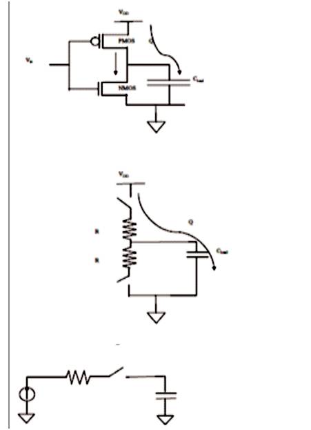
In conventional level-restoring CMOS logic circuits with rail-to-rail output voltage swing, each switching event causes an energy transfer from the power supply to the output node or from the output node to the ground. To reduce the dissipation, the circuit designer can minimize the switching events, decrease the node capacitance, reduce the voltage swing, or apply a combination of these methods. In all these cases, the energy drawn from the power supply is used only once being dissipated. To increase the energy efficiency of the logic circuits, other measures can be introduced for recycling the energy drawn from the power supply. A novel class of logic circuits called adiabatic logic offers the possibility of further reducing energy dissipation during the switching events, and the possibility of recycling, reusing, some of the energy drawn from the supply. To accomplish this goal, the circuit topology and the operating principles have to be modified, sometimes drastically. The amount of energy recycling achievable using adiabatic techniques is also determined by the fabrication technology, switching speed, and the voltage swing.The adiabatic logic structure dramatically reduces the power dissipation. Adiabatic logic offers a way to reuse the energy stored in the load capacitors rather than the traditional way of discharging the load capacitors to the ground and wasting this energy. Figure 1 shows the circuits’ Adiabatic switching.
Figure 1. Circuits Explaining Adiabatic Switching
The word Adiabatic comes from the Greek word that is used to describe thermodynamic processes that exchange no energy with the environment and therefore, no energy loss in the form of dissipated heat. In real-life computing, such ideal process cannot be achieved because of the presence of dissipative elements like resistance in a circuit. However, one can achieve very low energy engine dissipation by slowing down the speed of operation and only switching transistors under certain conditions. The signal energies stored in the circuit capacitances are recycled instead of being dissipated as heat. The adiabatic logic is also known as Energy Recovery CMOS.
The fully adiabatic operation of the circuit is an ideal condition which may be approached asymptotically as the switching process is slowed down. In most practical cases, the energy dissipation associated with a charge transfer event is usually composed of an adiabatic component and a non-adiabatic component. Therefore, reducing all the energy loss to zero may not be possible, regardless of the switching speed. With the adiabatic switching approach, the circuit energies are conserved rather than dissipated as heat. Depending on the application and the system requirements, this approach can sometimes be used to reduce the power dissipation of the digital systems.
When the first integrated electronic circuit was built on a single slice of Germanium by Jack Kilby in 1958 at Texas Instruments in Dallas, nobody knew that this invention will revolutionize electronics market, and consequently the life of everyday. Several decades later, Jack invention known as Integrated Circuits (ICs), is being used in a wide range of applications, from high-technology space crafts to small toys for kids. The ICs world is accustomed at this point to following the Moore's Law. In 1965,Gordon Moore observed that the number of transistors that can be most economically manufactured on a chip doubles every 18 months. Since that time, the IC industry has maintained the astonishing exponential trend, which Moore first observed, by continuing to scale down the size of transistors to have faster, cheaper, and less power consuming ICs (i.e., Dennard's Scaling Law).
The traditional goal has been to reduce the minimum feature size by 30% with each new technology. This scaling, theoretically, results in 30% and 50% reduction in logic gate's delay and chip area, respectively. Likewise, active power should decrease for a given circuit due to smaller transistors and lower supply voltages. Obviously, this scaling cannot go on forever because transistors cannot be smaller than atoms. Dennard Scaling Law has already begun to slow. In 1990s, experts agreed that the scaling would continue for at least a decade, but in 2009, they predicted that Moore's Law will continue for another decade. Despite the reduction of power consumption in each individual transistor caused by scaling, the total power consumption per chip has drastically increased due to the exponential growth in the number of integrated devices per chip and the increase in the clock frequency. A power consumption of 8 W is reported for an Intel Pentium CPU operating at 75 MHz, whilst the power consumption is increased to 150 W for a newer CPU generation, Core 2 Extreme QX9775 operating at 3.2 GHz. This increase in the power consumption that is noticeable in high- performance applications such as microprocessors, introduces new challenges to both fabrication and circuit design engineers, like the need for special packaging for the quick removal of the produced heat inside the chip and designing more stable circuits with respect to temperature variations inside the chip. Therefore, exploring design methodologies for low-power circuit is of great importance.
In addition to the heat problem, demands for portable battery-operated devices have increased significantly over the last decades. Taking a laptop as an example, consumers are strongly calling for laptops with lower price but much longer running time per charge. Furthermore, in some applications like implantable biomedical devices, where changing the battery needs a surgery, a small battery should work for tens of years inside the patient's body. Also, while the number of transistors integrated on a chip doubles every 18 months based on the Moore's Law, the capacity density of batteries doubles only every 10 years. Hence, the energy consumption becomes a bottleneck rather than the performance for many applications. All of this attention to the power and energy consumption in circuit design has created a significant research potential for minimizing or at least reducing the energy or power consumption. In the following, first, a brief history of ULP applications is presented. Then, the subthreshold operation is introduced as a solution for most ULP applications. The challenges in the design of subthreshold circuits are discussed next. Thereafter, the previous related sub-threshold work is reported to address how researchers have faced these challenges and studied the drawbacks of their researches.
There are many ULP applications that need small battery size and small amount of produced heat, especially in biomedical applications to prevent any damage to the tissues. It seems that lowering the supply voltage is the best solution to meet the requirements of such applications. Both energy and power consumption depend on the supply voltage, i.e., lowering the power supply will decrease both. Now, there is a question to be answered. What is the minimum limit of the power supply? Can we reduce the supply voltage indefinitely? Operating in this new range of supply voltage, which is less than transistors' threshold voltage, is referred as Sub-threshold operation. This mode of operation involves using a supply voltage in the 0.2 to 0.4 V range that is substantially lower than the nominal supply voltage (which fall in to the 0.9 to 1.2 V range) for the modem CMOS technologies. Decreasing the power supply reduces both the active and static consumed power by a circuit.
The two existing low-power technologies to be considered for lower power consumption are sub-threshold CMOS theory and adiabatic logic circuit technology. Subthreshold CMOS theory is a technique which can reduce the power consumption to lower than threshold voltage. On the other hand, adiabatic logic circuit is a technique that varies the slope of the constant voltage power supply, and it reduces energy consumption by suppressing the voltage applied to the resistance of the circuit.
A sub-threshold adiabatic logic circuit uses two power supplies which have different frequencies and power supply, and therefore the power consumption of the proposed logic is reduced ( M. Khatir, H. G. Mohammadi, and A. Ejilali, 2010). The Two Phase Clocking Subthreshold Adiabatic Logic (Kazunari Kato, Yasuhiro Takahashi, and Toshikazu Sekine, 2014) uses a two phase clocking power supply which uses two different frequency and amplitude. For example, a 2-chain inverter circuit is shown in Figure 2. The timing chart for the circuit is shown in Figure 3. It is necessary to switch on-off the input signal when the frequency is of twice, based on the frequency of , and the input signal frequency is 1/2. The amplitude of and are 0–0.5V and 0–0.25V respectively. The frequencies of and are 10kHz and 20kHz. In period of T2, T4, T6 and T8, the voltage of these power supplies is low level and therefore, the outputs are always low-level; this means these timing become read protection period.
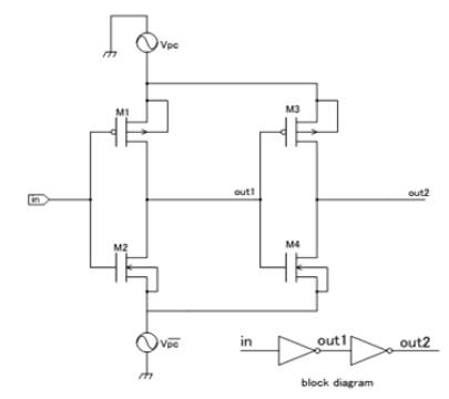
Figure 2. Cascaded inverter
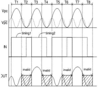
Figure 3. Timing chart for cascaded inverter
Sub-threshold operation seems the best match for ULP applications as their usage is daily increasing. However, there are some challenges that sub-threshold designs face. Sub-threshold researches are focused on overcoming these challenges. These challenges are discussed in the following.
1) When the supply voltage drops below the threshold voltage, the transistor current still remains above zero. A nonzero gate-to-source (Fgs) voltage that is less than transistor threshold voltage still produces a current that is larger than the off-current, /0fr ( i.e., the transistor current when Fbs=0 V). This finite ratio of the on-current,70n, to 70ff lets sub-threshold digital gates behave statically in a similar fashion to the super-threshold gates. However, their transient behavior is much slower than the super-threshold ones, due to the small drive currents. The frequency of operation in the sub-threshold region is orders of magnitude smaller than that of the super-threshold region. For instance, Figure 3. (top) shows that reducing the power supply from its nominal value, 1.1 V, to the subthreshold value, 0.2 V, reduces the operating frequency by three orders of magnitude for about 20 times reduction in the total energy per operation.
2) As shown in Figure 3. (bottom), the I0J I0ff ratio reduces about three orders of magnitude when the supply voltage reduces from its nominal value to the subthreshold value. This reduction in the / on/ off ratio can lead to reliability problems. For example, for certain gates with parallel leaking path (e.g., NOR).
3) Process-Voltage-Temperature (PVT) variations that become more prominent in modem CMOS technologies, affect the transistor threshold voltage and consequently the current, both in the super-threshold and sub-threshold regions. However, this effect is more obvious in the sub-threshold region because of the exponential relation between the current and threshold voltage (i.e., 1D ocexp (Vcs — Vth), where V&is the threshold voltage of transistor). Despite the mentioned challenges, researchers have successfully developed techniques to build relatively fast and robust sub-threshold digital circuits ranging from small gates and SRAMs to processors. Overcoming these challenges needs a wide collaborative research at every design hierarchy level.
Some of the important research topics are listed below.
Standard transistors are super-threshold transistors and optimized for operation in their nominal supply voltages for high-performance applications. It is an established fact that the doping profile and level in conventional transistors are designed to mitigate the Short-Channel- Effects (SCE), e.g., punch-through. However, in the subthreshold region, the supply voltage is small and SCEs are not significant. It means that many of the process steps to produce special drain and source region or channel doping tuning are not any more necessary for transistors operating in the sub-threshold region. On the other hand, the gate oxide thickness should be optimized for this region of operation. Reducing the oxide thickness does not always impose a positive effect in sub threshold operation. Reducing the oxide thickness decreases the sub-threshold slope, which is desirable for this mode of operation, and in parallel, increases the gate capacitance that causes more delay and energy consumption. Hence, the oxide thickness should be optimized for subthreshold operation. Also, a new transistor structure, called the Double GateMosfet, is introduced for sub-threshold operation, that shows a more ideal sub-threshold slope. In this kind of transistors, a longer channel length can be used to have more robust ULP circuits.
Unlike the super-threshold, where good and valid models are established for current and capacitances, in the subthreshold region there is a need to model transistors.
There is a great need to speed up sub-threshold circuits to expand ULP circuits applications to higher frequencies. A conventional method to increase the speed of a circuit in the super-threshold region is to increase manipulating the channel width of the transistors through applying the method of logical effort. Such methods are very powerful as long as digital circuits operate in the super-threshold region. However, applying logical effort for sub-threshold operation is quite different, because the current may not show a linear relation with the channel width. On the other hand, in most super-threshold circuits, the channel length is set to its minimum value. But, it has been shown that increasing the channel length to few folds of its minimum value improves the performance of circuits operating in the sub-threshold region.
Some of the circuit topologies that operate well under the super-threshold conditions might not be suitable for operating in the sub-threshold region, and vice versa. For example, pass-transistor-logic (PTL) families suffer from a threshold voltage drop in the super-threshold operation. To overcome this issue, keepers or transmission gates are introduced that increase the number of transistors and, as a result, the power consumption. Whilst, in the subthreshold region, there is no threshold voltage drop. Reduced IotJI0« ratio in the sub-threshold region forces the designer to design more robust circuits. Some introduced techniques cannot be used in the superthreshold. For instance, Dynamic- V&-CMOS (DVTCMOS) uses transistors with gate and body tied together. DVTCMOS has the same characteristics as a conventional MOSFET in the “off ” state. But, in the “on” state, the threshold voltage reduces producing a larger on-current. This improves the /on//off ratio. Sub-threshold logic circuits are slow and make these circuits more suitable for adiabatic computation. Many studies have been performed on XOR gates, adder circuits, and some fundamental blocks used in sub-threshold digital circuits.
While energy minimization is not of primary importance for high-performance systems operating in the superthreshold region, it is a major topic in the sub-threshold design. Sub-threshold design has been introduced to meet the energy constraints in ULP applications. Hence, the designer in this area should be aware of the effect of different variables like Fdd, Fth, and transistor sizes. Inanalytical models are introduced to find the optimal Fdd, Fth, and transistor sizes to obtain the minimum energy consumption.
Energy-efficient sub-threshold design cannot succeed without robust and dense SRAMs. SRAM is an important component of many ICs, and it can contribute a large fraction of the active and static energy. The widely used 6T SRAM cell fails to operate in sub-threshold. Reduced 7on//off ratio complicates the reading and writing steps in the sub-threshold region. So, it is important to have SRAMs compatible with the sub-threshold systems. Some samples of research are on sub-threshold SRAMs.
Since an entire system may not be able to operate completely in the sub-threshold region, there is a need for periodic switching between the nominal supply voltage and sub-threshold supply voltage, Also, connecting different parts of a system operating in different voltages needs DC/DC level converters. In addition, pipelining and parallel architectures can increase the speed of sub-threshold circuits. Although, no commercial applications have yet adapted this approach, it is expected that subthreshold and near threshold circuits will make their way into commercial products.
In the RESET (rst) phase the inputs are low, the outputs are complementary (one high, the other low), and the power supply ramps down. In the WAIT (second) phase, the power-supply stays low, maintaining the outputs low and the inputs are evaluated. Note that because the gate is powered down, the evaluation of the inputs will have no effect on the state of the gate. In the EVALUATE (third) phase, the power supply ramps up and the outputs will evaluate to a complementary state. At the end of EVALUATE, the outputs will always be complementary. In the HOLD (fourth) phase, the power supply clock stays high while the inputs ramp down to low. Gate outputs remain valid for the entire phase as shown in Figure 4.
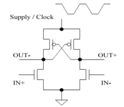
Figure 4. Basic 2N-2P differential buffer/inverter
A variant on the 2N-2P logic family described above is that of the 2N-2N2P family, the only difference being that 2N- 2N2P has a pair of cross-coupled Nfets in addition to the cross-coupled Pfets common to both families (Figure 5). 2N-2N2P thus has cross-coupled full inverters and thus is very similar to a standard SRAM cell. The timing and logical operation of 2N-2N2P is identical to that of 2N-2P.
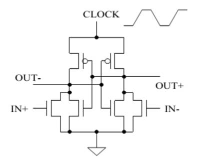
Figure 5. 2N-2N2P Inverter Gate
The primary advantage of 2N-2N2P is that the cross coupled NMOS transistors result in non-floating output for large part of the recovery phase. The drawback of the 2N- 2N2P gate is that it requires four phase clocks. Figure 6 shows 2N-2N2 Inverter for timing.
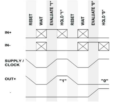
Figure 6. Timing for 2N-2N2P Inverter
ECRL has the same circuit structure as cascade voltage switch logic (CVSL). Figure 7 shows ECRL Inverter and clock. Assume that 'in' is at high and 'inb' is at low. At the beginning of a cycle, when the supply clock Ψ1 rises from zero to VDD, out remains at a ground level because 'in' signal turns on MN2.Outb follows Ψ1 through MP1. When Ψ1 reaches VDD, the outputs hold valid logic levels. These values are maintained during the hold phase and used as inputs for the evaluation of the next stage. After the hold phase,Ψ1 falls down to ground level, outb node returns its energy to Ψ1 so that the delivered charge is recovered. Thus the clock Ψ1 acts as both a clock and power supply. Wait phase is inserted for clock symmetry. In this phase, valid inputs are being prepared in the previous stage.
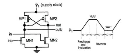
Figure 7. ECRL Inverter and clock
Figure 8 shows phase relationship among supply clocks. ECRL uses four-phase clocking to efficiently recover the charge delivered by the supply clock. Each clock is followed by the next clock with a 90o phase lag. So when the previous stage is in the hold phase, the next stage must evaluate logic values in the precharge and evaluation phase.
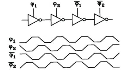
Figure 8. Inverter chain and four phase
Output and clock waveforms of a inverter chain and energy dissipation are shown in Figure 9. ECRL logic will offer high operation speed. The drawback is that it requires push-pull operation and four phase driving.
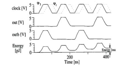
Figure 9. Node waveforms of Inverter chain supply clock
The inverter stage of the CAL is shown in Figure 10. The cross coupled M1-M4 provides memory function. The circled devices M5, M6 can be replaced with NMOS logic trees to perform more complex complementary logic functions on the true (F0) and the complementary (F0) logic inputs. Idealized CAL timing waveforms are shown in Figure 11. The power clock PCK is shown as a 0 to VDD trapezoidal waveform. In the clock period A, the auxiliary clock CX enables the logic evaluation. For F0 = 0, M8 and M6 are on, F1 = 0, M1 is on and the output F1 closely follows the power clock waveform. In the next clock period B, the auxiliary clock CX = 0 disables the logic evaluation.
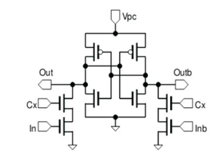
Figure 10. CAL Inverter
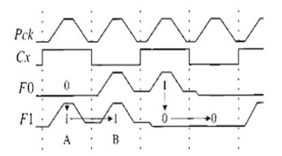
Figure 11. Timing waveform
In order to use one-phase driving, this type of adiabatic logic includes NMOS transistors controlled with auxiliary clock pulse CX. On the other hand, the generation of the auxiliary clock (with a frequency divider) means spending more power.
The advantage is that it is possible to achieve quasiadiabatic operation with conventional static CMOS gates under one-phase driving. On the other hand, the disadvantage is that the output node is to be floating from the effect of the split-level driving clocks.
The operation of the P-ECRL circuits can be divided into four processes: evaluation (t1 ), hold (t2 ), recovery (t3 ) and wait phases (t4 ). Let us assume 'in' is at high and 'inb' is at low at the beginning of a cycle, and so that out is clamped to VDD . During the evaluation phase, as the clock clk1 goes down, the output outb goes low via N1 by the falling clk1 . When clk1 reaches GND, the outputs hold valid logic levels. These values are maintained during the hold phase and used as inputs for evaluation of the next stage. After the hold phase, clk1 goes up to high level, and outb node returns its energy to clk1 , so that the delivered charge is recovered. Wait phase is inserted for clock symmetry. In this phase, valid inputs are prepared in the previous stage. When the previous stage is in the hold phase, the next stage must evaluate logic value in the evaluation phase. Figure 12 shows PECRL schematic.
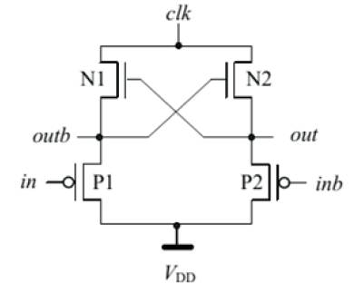
Figure 12. PECRL schematic
It consists of three main parts:
The advantage of Two Phase Clocked CMOS Adiabatic Logic (2PC2AL) is that it is possible to achieve quasiadiabatic operation with conventional static CMOS gates under one-phase driving. Figure 13 shows the timing chart. It requires split-level driving clocks. The disadvantage is that the output node is floating from the effect of the split-level driving clocks. Figure 14 and 15 show the SAL inverter and 2PC2AL Inverter and its clock.
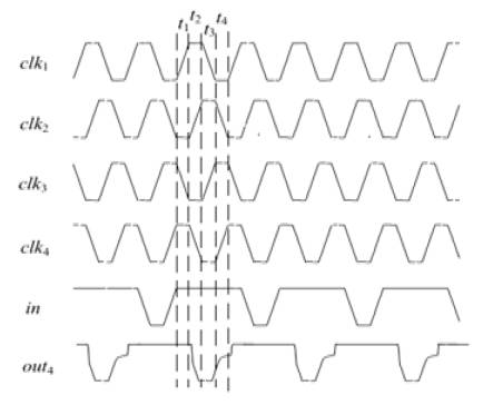
Figure 13. Timing chart
Figure 14. SAL Inverter
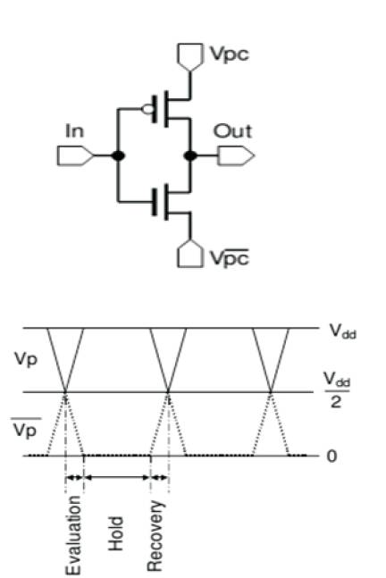
Figure 15. 2PC2AL Inverter and its clock
Fundamental and the core of all the Digital Signal Processors (DSPs) are its multipliers and speed of the DSPs is mainly determined by the speed of its multipliers. Multiplication is the most fundamental operation with intensive arithmetic computations. Two important parameters associated with multiplication algorithms performed in DSP applications are latency and throughput. Latency is the “real delay of computing a function”. Throughput is a measure of “how many computations can be performed in a given period of time”. The execution time of most DSP algorithms is dependent on its multipliers, and hence need for high speed multiplier arises. Digital signal processing (DSP) is the technology that is omnipresent in almost every engineering discipline. It is also the fastest growing technology this century and, therefore, it poses tremendous challenges to the engineering community. Faster additions and multiplications are of extreme importance in DSP for convolution, discrete Fourier transforms, digital filters, etc. The core computing process is always a multiplication routine; therefore, DSP engineers are constantly looking for new algorithms and hardware to implement them. The exploration of Vedic algorithms in the DSP domain may prove to be extremely advantageous.
In many DSP algorithms, the multiplier lies in the critical delay path and ultimately determines the performance of algorithm. The speed of multiplication operation is of great importance in DSP as well as in general processor. In the past, multiplication was implemented generally with a sequence of addition, subtraction and shift operations. There have been many algorithms proposals in literature to perform multiplication, each offering different advantages and having tradeoff in terms of speed, circuit complexity, area and power consumption. The multiplier is a fairly large block of a computing system.
Multiplication Algorithms show a great effect on the processors' performance. Multiplier is an important block used in electronic industry, especially in Digital Signal Processing operations such as filter design, convolution and analyzing of frequency. There are different types of methods used in multipliers to increase the performance. To evaluate the functionality and performance of 4×4 array multiplier, it used Sixteen ANDs, six full adders, four half adders and eight D flipflop as show in Figure 16. In this figure, a0 to a3 and b0 to b3 are the inputs and p0 to p7 are the outputs. The figure demonstrates the input and output waveforms of 1 kHz transition frequency.
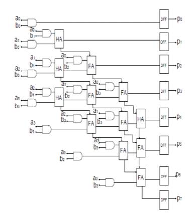
Figure 16. Conventional 4 X 4 Array multiplier
Jagadguru Swami Sri Bharati-Krishna Swamiji introduced his research on mathematics based on different sutras for multiplication design. A multiplier is the Key block in Digital Signal processing systems. Now a days, researchers are trying to design different multipliers which offer good computational speed, less delay, low power and area efficient. (Jagadguru Swami Sri Bharati Krishna Tirthji Maharaja,1986)
The multiplication is per formed using Urdhva- Tiryagbhyam Sutra of Vedic mathematics (A.P. Nicholas, K.R Willaiams, J. Pickles, 2003). The Comparison between number of multiplications and additions in Conventional Mathematical approach and vedic mathematics is shownbelow . (Human Tharafu M.C. Jayalaxmi. H. Renuka R.K Ravishankar. M.,2007).
Vedic Mathematics offers a fresh and highly efficient approach to mathematics covering a wide range. This book starts with elementary multiplication and concludes with a relatively advanced topic, the solution of non-linear partial differential equations. But the vedic scheme is not simply a collection of rapid methods: it is a system, a unified approach, which can be swiftly learnt (Purushottam D. Chidgupkar and Mangesh T. Karad,2004). Let input sequence be a[n]={a3,a2,a1,a0} and b[n]={b3,b2,b1,b0}
The multiplication of a[n] and b[n] is given by y[n]={P0,P1,P2,P3,P4,P5,P6} and is calculated by
P0=a0*b0
P1=a0*b1+a1*b0
P2=a0*b2+a1*b1+a2*b0
P3=a0*b3+a1*b2+a2*b1+a3*b0
P4=a1*b3+a2*b2+a3*b1
P5=a2*b3+a3*b2
P6=a3*b3
Consider computing the product of two 4-bit integer numbers given by A3A2A1A0(multiplicand) and B3B2B1B0 (multiplier). The product of these two numbers can be formed as shown below.
Each of the AND terms is referred to as a partial product. The final product (the result) is formed by accumulating (summing) down each column of partial products. Any carries must be propagated from the right to the left across the columns. (Human Tharafu M.C. Jayalaxmi. H. Renuka R.K. Ravishankar. M.,2007)
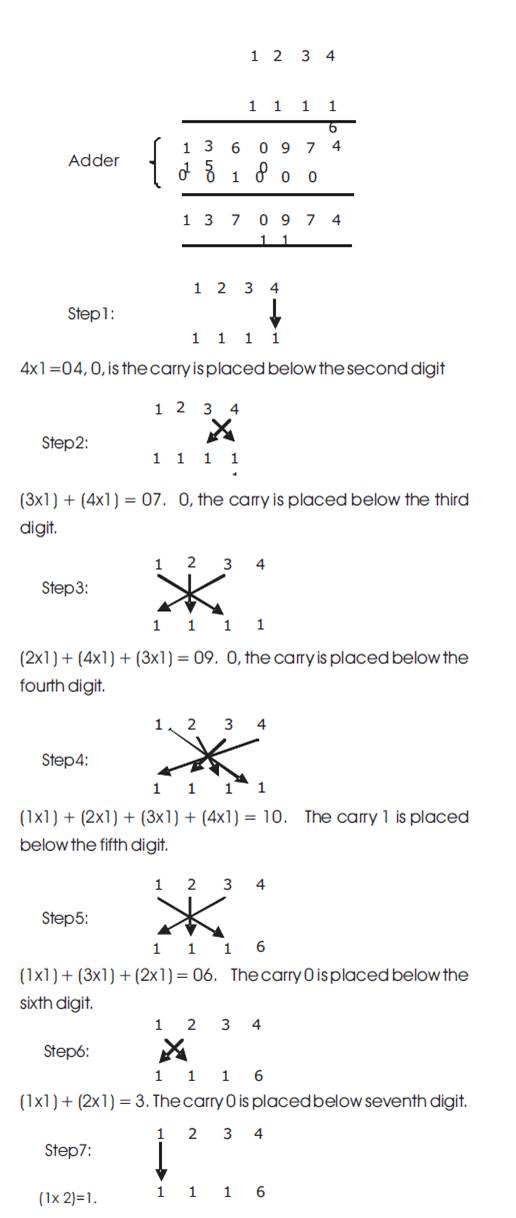
Since dealing with binary numbers, the partial products reduce to simple AND operations between the corresponding bits in the multiplier and multiplicand. The sums down each column can be implemented using one or more 1-bit binary adders. Any adder that may need to accept a carry from the right must be a full adder. If there is no possibility of a carry propagating in from the right, then a half adder can be used instead, if desired (a full adder can always be used to implement a half adder if the carry-in is tied low).Example: Multiplication of 1234 and 2116. Figure 17 shows Vertical and Crosswise Sutra.
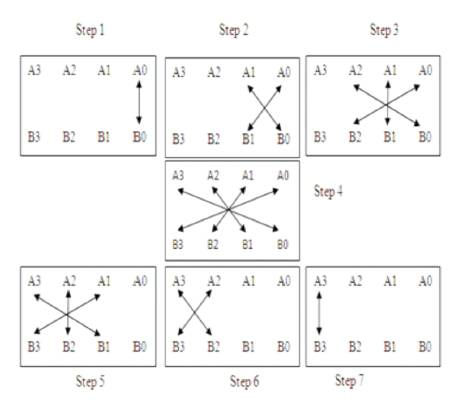
Figure 17. Diagram of Vertically and Crosswise Sutra
In this paper, Figures 18,19 and 20 are showing the simulation results for 4 X4 conventional multiplier,4 X 4 adiabatic two phase multiplier and 4x4 Array Multiplier using Subthreshold Adiabatic logic using Vedic mathematics.
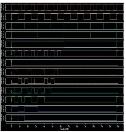
Figure 18. Output waveform for 4x4 Array Multiplier using CMOS logic
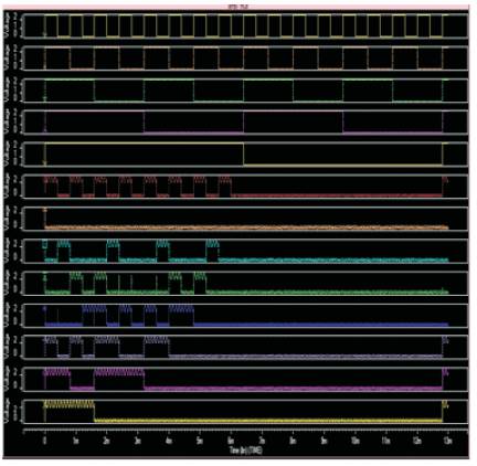
Figure 19.Output waveform for 4x4 Array Multiplier using Subthreshold Adiabatic logic
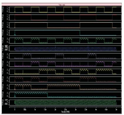
Figure 20.Output waveform for 4x4 Array Multiplier using Subthreshold Adiabatic logic using Vedic maths
The conclusion of this paper was to introduce a method for calculating the multiplication between two numbers of finite length numbers that is easy to learn and perform. The power dissipation using Vedic multiplication algorithm is compared with that of conventional multiplication which is less. There is a considerable improvement in their performance as compared to traditional method of implementation.
In this paper, Table1 shows the power dissipation calculation. The proposed circuit has used two different frequency and amplitude power supply. Then we have functionality operation of these circuits by SPICE simulation and also the authors have compared power dissipation with conventional CMOS multiplier. Key element behind increasing speed of multiplier design is based on UrdhvaTir yagbhyam sutra of Vedic mathematics and parallel implementation of hardware. Vedic Mathematics is like drops picked up from the ocean of Vedas. The exploration of Vedic algorithms in the DSP domain may prove to be extremely advantageous. This paper can extend to DSP applications such as convolution and correlation concepts.
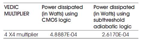
Table1. Power dissipation calculation