(1)

IC Designers are struggling for tradeoff between significant variation effects and very tight power constraints in current nanometer regime. Usage of conventional timing safety margin approach becomes the cause of continuous power consumption to prevent the design from low probability timing variations. Various solutions have been proposed to achieve optimized power consumption/dissipation. Dynamic Threshold Voltage Vth Scaling (DVTS), Dynamic Voltage Scaling (DVS) and Dynamic Voltage and Frequency Scaling (DVFS) are some of the reported techniques in literature to achieve optimized power consumption. These approaches deals with aggressive standby Vth and VDD scaling by tracking PVT variations to smartly tradeoff between safety of data and decreased power consumption. In this paper different power saving strategies are discussed along with their benefits and limitations. This study will be helpful to select an effective power saving strategy to minimize the power dissipation.
Nowaday's most critical concern in sub threshold circuits is to achieve high level of performance with very tight power constraints. Power has emerged as the most important figure of merit for designs beyond the 65nm generation. The performance of submicron circuits is very sensitive to manufacturing and environmental variations due to the exponentialdependency on threshold voltage (Vth), supply voltage, capacitive power dissipation and operating frequency. There are mainly two approaches to address power dissipation in sub-micron circuits. In this paper these approaches are discussed and reviewed in detail along with their limitations and advantages.
The power dissipation of a sub-micron circuit may be given as below
Where,
CL : Capacitive Loading, Vdd : Voltage Swing, f: Frequency, a: Activity factor (statistical factor)
Based on equations (1) and (2) this paper presents different techniques to optimize the power dissipation in the circuit. These techniques are
(i)Dynamic threshold voltage Vth, scaling DVTS [1-2].
(ii)Dynamic Voltage Scaling (DVS) [3-4] and Dynamic Voltage and Frequency Scaling (DVFS) [5].
To achieve higher integration density and performance sub-threshold circuits have been scaled down aggressively. This leads to a higher leakage with technology scaling and became significant contributor to total power dissipation. To deal with these issues by excessive guard bands, became very difficult because of the random process variations. Estimation and control of leakage current dragged major attention of the designer, major contributors of the leakage current can be broadly classified as
All these components increase drastically in scaled devices resulting in a huge increase in cumulative leakage current. Each component depends on the transistor geometry: (gate length (Lg), width (W), oxide thickness (Tox ), junction depth (Yj), Source-Drain extension length (LSDE),), the doping profile (channel doping (Ndep ) and “halo” doping (Npocket) concentration), the flatband voltage (Vfb ), and supply voltage (Vcc) [2-3]. Various methodologies have been proposed to minimize leakage, which are discussed Section 2.
Traditionally, the most common practice is to handle power by guarding normal circuit delay with safety margins in timings. Due to variations in uncertainty, designers need to use pessimistically very large margins [3-5] for safety in designs and to guarantee the correct functionality under worst case variations. This over constrain design not only slows down the performance but also causes excessive power dissipation. As the possibilities of these worst cases are less but more power is consumed continuously to maintain the safety guards. Moreover, these type of safety guards are not efficiently used during the life cycle of a design. Hence power usage is not as efficient as per the call of the time. Different DVS and DVFS techniques [6] proposed by various authors are given in Section3. There are some more traditional techniques which are explored up to their best performance level and are presently very stable, so these are kept out of scope of this paper like
Different techniques proposed w.r.t. the requirements to reduce the leakage current. Sub-threshold circuits are commonly designed to perform with highest efficiency, realized with complex gats and parallel architecture with duplication of logic. Some logic of the design is not expected to perform at their highest level of efficiency all the time. This part of the design can help to reduce the leakage power without impacting the overall performance of the design. By controlling the leakage 30 to 40% of power dissipation is reported by different researches. This issue has been addressed in two ways
These are the techniques which uses the delay slack in non-critical paths for leakage reduction. As these techniques are static so cannot be changed at run time. High Vth CMOS transistors have less leakage and vice- versa, so by assigning high Vth transistors to the non-critical path can reduce the leakage. On the other hand using low Vth transistors in the critical paths efficiency is also not compromised [2], [7]. High efficiency and low leakage can be achieved without any extra circuitry requirement. Apart from this, dual threshold transistors are capable of reducing leakage power in standby and active mode as well [8]. Due to increasing variation in Vth and supply voltage scaling, it is more difficult to achieve sufficient gap among low Vth, high Vth and required supply voltage for dual Vth design. However, the dual Vth design increases the number of critical paths.
When the power dissipation is controlled through DVTS technique on the fly or run time are classified as run time techniques.
Some times when the critical part(s) of the design are not required to be active, kept in stand-by mode to reduce its leakage power. These various standby techniques proposed for leakage reduction are discussed below
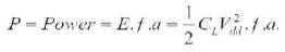
For Negative Channel MOS (NMOS) or Positive Channel MOS (PMOS) transistors leakage current depends on the voltage at the four terminals (Source, Drain, Gate and Substrate) of transistor. NMOS transistor reduces subthreshold leakage current exponentially with increase in source voltage due to negative Vgs. Lowered signal rail (Vcc-Vs), reduced Drain Induced Barrier Lowering (DIBL)[1], [3] and body effect is named as self-reverse biasing of transistor. Self-reverse bias effect achieved by turning off a stack of transistors [9]. Source acts as reserve biasing when more than one transistor in a stack is turned off, raises internal source voltage of the stack, which acts as reverse biasing the source as shown in Figure 1.
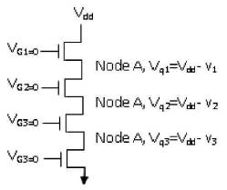
Figure 1. Transistor Stacking Diagram
Gate and junction leakage also have importance in scaled technologies, controlled input vector technique using a stack of transistors needs to be adopted carefully to reduce the total leakage in an effective manner. Traditional way of stacking fails to reduce leakage and at the worst case corner may increase the overall leakage.
Extra, series connected transistor called sleep transistor in the pull-down and pull-up paths of a gate and turn them 'off' in the standby mode of operation [10]. In regular mode, the extra transistor is turned on. It provides substantial savings in leakage current during standby mode of operation. Due to the extra sleep transistor, the drive current of forced-stack gate is reduced, resulting in increased delay. So, this technique can be only adopted for non-critical paths. With high Vth of the sleep transistor, extra leakage saving is possible. This circuit topology is known as MTCMOS [2], [11] Figure 2.
Practically, either PMOS or NMOS with high Vth transistor is sufficient to reduce leakage. Preferably NMOS insertion scheme is preferred, since the on resistance of NMOS is smaller with same width, so NMOS can be sized smaller than a corresponding PMOS [12].
Figure 2. Low Vth Device MTCMOS Circuit Schematic
CMOS with Variable threshold is a body biasing design technique named as Variable Threshold CMOS (VTCMOS) [13] as shown in Figure 3(a) [2]. To achieve different threshold voltages, body bias is controlled by selfsubstrate bias circuit. In active mode Zero Body Bias (ZBB) is applied. In standby mode, to cutoff the leakage current and to increase Vth a deep Reverse Body Bias (RBB) is applied. To apply body bias voltage it requires routing a body bias grid and leads to add the overall silicon size. It was reported by Keshavarzi et. al. that RBB lowers IC leakage by as much as three orders of magnitude in a 0.35 m technology [14].
In scaled technologies, recently it is proposed to use forward body biasing named FBB [15] to achieve better current drive with lesser short channel effect. In standby mode circuit is designed using high Vth transistor reducing leakage, while in active mode FBB is adopted to achieve higher performance.
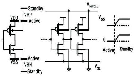
Figure 3. (a) Variable threshold CMOS, (b) Realizing body biasing by changing the source voltage with Zero body Voltage
As we know every application does not require a high performance circuit all the time. This idea is exploited in active leakage techniques to intermittently slow down the fast circuitry to reduce the leakage power consumption and the dynamic power consumption as well when maximum performance is not expected.
In DVTS scheme body biasing is used to adaptively change the threshold voltage Vth as per the performance demand. For highest performance requirement lowest Vth (NBB – No Body Bias) is delivered. When performance demand is not expected to be high, clock frequency is reduced and Vth is increased by RBB to reduce the leakage power. When there is no workload, Vth can be raised to its maximum value to reduce the standby leakage power significantly. By tracking the optimal Vth “Just enough” throughput is delivered for current workload while leakage power is reduced enough by intermittently slowing down the circuit.
Different DVTS system implementations have been proposed in [16-17]. Figure 4 shows DVTS architecture, using continuous body bias control for tracking the optimal Vth for a given workload [2]. A clock speed controller embedded in the operating system, determines the run-time (reference) clock frequency requirement. PMOS and NMOS body bias is controlled through DVTS in a way that oscillator frequency of replica of critical path tracks the given reference clock's frequency. Difference between the reference clock frequency and the oscillator frequency, generates the error signal and is used in the feedback controller.
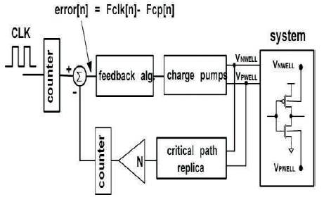
Figure 4. DVTS Architecture
Figure 5 represents the relation between performance and supply voltage while Figure 6 shows the relation between power consumption and supply voltage.
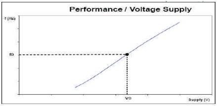
Figure 5. Performance v/s Supply Voltage
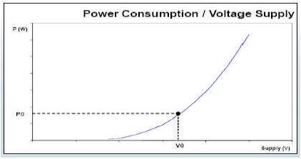
Figure 6. Power Consumption v/s Supply Voltage
Now it is clear to control supply voltage for power dissipation reduction there are techniques proposed like DVS and DVFS. In case, circuit is not able to support the desired output at some voltage level due to the timing violation, desired boost can be given by scaling up the supply voltage of the circuit to behave correctly. Therefore, the voltage level is only scaled up when the circuit is functioning at worst PVT conditions while, during normal operating conditions, the voltage level is kept as low as possible to save the power consumption [18-19]. Reduction of 40% to 50% in power dissipation is reported by different research using DVS and DVFS techniques. To decide when to step-up and when to step-down the supply voltage several techniques have been proposed these are
Razor technique eliminates the power inefficiency in a way that the design works at normal power consumption unless until not required to consume more power [24-27]. The peak power required in the worst case is only used when it is required. A broad level schematic and typical circuitry can be understood by Figure 7.
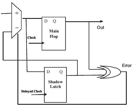
Figure 7. Razor Flop Schematic
As from the above circuitry it is clear that it works on the error detection and correction basis. Error is the output of the comparator logic, where the actual Flip Flop out is compared with the shadow FF output, which is supposed to give a correct output due to its delayed clock. We know that the typical worst case operations are limited, so the probability of error is also limited. Because of this the requirement of error correction is also less hence the saved power can be used for error correction.
Timing elasticity is the extension of the Razor application where the clock period of the main Flip Flop is stretched [28], whenever the comparator output is seen 'high'. This way the probability of setup timing violation is avoided and power is saved.
There were few limitations of the Razor Technique which were addressed with the help of some modifications in the originally proposed circuit [29]. In this case when error signal is generated at comparator output, it is used to select the correct output of shadow FF through muxing logic. The schematic of this modified razor can be understood by Figure 8.
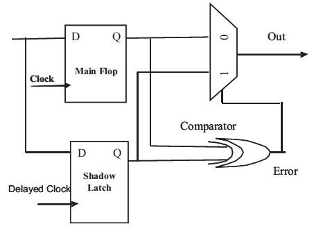
Figure 8. Modified Razor Flop Schematic
Even after these modifications Razor Technique, it is not efficient technique for all kind of circuits. Especially, for the circuits having some pipeline stages this methodology became very difficult to implement. Because in these cases either it is required to have duplication as recovery circuit needed or to flush out the whole pipeline stage. In both of the cases it was not been an efficient method w.r.t. the circuit overhead and time frame.
As discussed above the limitations of the Razor flip flop [30]. there is still a scope to have more efficient method to deal with all kind of the circuits. To address this limitation, canary technique was proposed, where there was no need of any re-execution of any step/stage, therefore, the requirement of any duplication of the circuit is no more needed [31]. Canary technique works on the basis of early warning methodology [32-33] and gives sufficient time to take the corrective actions, if there is any timing violation is about to happen at main FF. The circuit diagram given in Figure 9 explains itself its functionality.
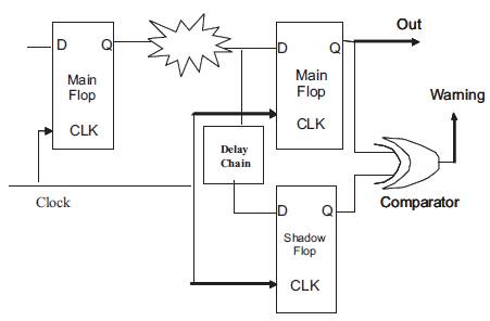
Figure 9. Canary Flip-Flop Schematic
It is evident from the schematic that it works on the basis of early prediction of the error so the output of the comparator is named 'warning' signal. In this Technique some delay element is added before the D input of the shadow flip flop (called Delay Chain) by which any setup timing violation will occur at the shadow FF earlier to the main FF. As there is no need of any corrective action to be taken at functionality level so the need of circuit duplication is easily avoided. This warning signal is used to handle incorrect output of the circuit, accordingly.
As shown in Figure 10 each Flip-Flop of main DUT is tracked with its individual shadow FF. Each Canary Flip-Flop or Razor Flip-Flop is a combination of comparator and a configurable delay chain in data path or a delayed clocked Flip-Flop respectively. Each comparator output is traced in monitor and speed control unit. Monitor and speed control unit selects minimum sufficient supply voltage to adaptively control the power consumption.
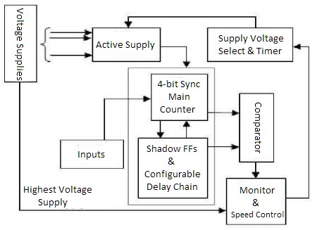
Figure 10. Block Diagram of Adaptive Technique
As discussed various techniques in this paper each one has its own benefits and limitations. Vth adaptive techniques acts as multiple pole closed loop control system which is difficult to act as stable system. Not only stability but also due the large bulk and triple well requirement it is not a cost effective solution. These issue demands further analysis and more effective solution to have more reliable, stable and a cost effective solution.
As for as DVS and DVFS techniques are concern there is no automated solution or support is available from Electronics Design Automation (EDA) industry which can make their implementation to be fast and hassle free. Some more work is expected on the requirement of high level characterization required for delay chain cells and timing margins required in Canary technique which is capable to predict and correct the timing error.
In the current deep sub-micron devices with low threshold voltages, sub-threshold, gate and junction leakage have become the dominant sources of leakage and are expected to increase with technology scaling. Low power supply with increasing circuit density and operating frequency are another dominant factor of sub-micron designing. Paper reviews different techniques of subthreshold circuits aiming at the per formance improvement of performance indices namely leakage power, error detection, error prediction, frequency adjustment e.t.c. Finally, process variation, its impact on leakage and various solutions to compensate process variation along with other adaptive techniques to reduce power dissipation are discussed. In some leakage reduction techniques nearly 30% to 40% power dissipation saving is reported and through DVS and DVFS nearly 40% to 50% of power dissipation is achieved.