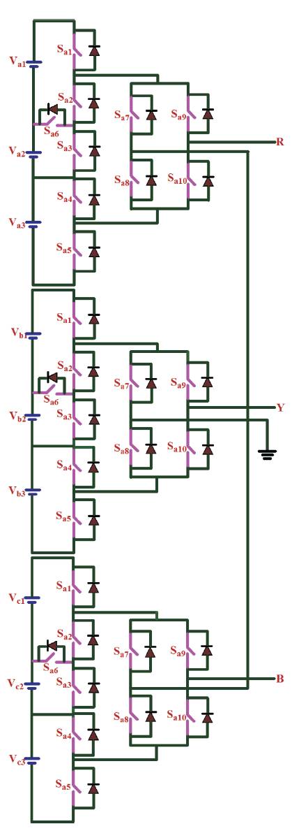
Figure 1. Three Phase Seven Level Inverter
Multilevel Inverters have been widely used for high power and high voltage applications as their performance is highly superior to that of conventional two level inverters due to reduced harmonic distortion, lower electromagnetic interference, and higher dc link voltages, but it has some disadvantages such as increased number of components, complex pulse width modulation control method and voltage-balancing problem. In order to compensate the above described disadvantages a new topology with a reversing voltage component is proposed to improve the multilevel performance. This topology requires fewer components compared to existing inverters (particularly in higher levels) and requires fewer carrier signals and gate drives. Therefore, the overall cost and complexity are greatly reduced particularly for higher output voltage levels. Finally, a prototype of the seven level proposed topology is built and tested with different modulation strategies to show the performance of the inverter by experimental results using MATLAB-SIMULINK. By comparing the various PWM techniques, it is observed that UAPODPWM provides less THD, and UCOPWM techniques provide higher fundamental RMS output voltage.
Multi Level Inverter (MLI) is a power electronic system that produces a desired sinusoidal output voltage from several levels of DC input voltages. Conventional two level voltage source inverter normally produces output voltage with zero (or) positive and negative voltage levels. It suffers from many disadvantages while operating at high frequency mainly due to losses and device ratings of semiconductor switches. To obtain the quality output with less distortion at high switching frequency, multilevel inverters with various PWM strategies are introduced and comparisons are made to chose the better strategy. The general concept involves utilizing a higher number of active semiconductor switches to perform the power conversion in small voltage steps. There are several advantages to this approach when compared with the conventional power conversion approach. The smaller voltage steps lead to the production of higher power quality waveforms and also reduced voltage (dv/dt) stress on the load and the electromagnetic compatibility concerns. Caballero et al [1] made a survey on new asymmetrical hybrid multilevel voltage inverter. Rahim et al [2] developed the transistor-clamped H-Bridge based cascaded multilevel with new method of capacitor voltage balancing inverter. Suroso and Toshihiko Noguchi [3] made a detailed review of multilevel voltage-Source inverter Using H-bridge and two-level Power modules with a single power source. Murugesan et al [4] presented a survey on new multilevel inverter topology using less number of switches. Santhi and Kannabhiran [5] carried out survey on new 81 level inverter with reduced number of switches. Gupta and Jain [6] performed a topology for multilevel inverters to attain maximum number of levels from given DC sources. Bayat and Babaei [7] found a Performance of new cascaded multilevel inverter with reduced number of switches. Sun et al [8] made a study on Performance of multi-level inverter capable of power factor control with DC link switches. Roshankumar [9] evaluated performance of a five-level inverter topology with single-DC supply by cascading a flying capacitor inverter and an H-Bridge. Ebrahimi et al[10] described a new multilevel converter topology with reduced number of power electronic components. Parker et al [11] proposed the distributed control of a fault tolerant modular multilevel inverter for direct drive wind turbine grid interfacing.
Multilevel voltage source inverters are used to increase the number of voltage levels, power rating and allows them to reach higher fundamental RMS voltage with relatively low harmonics without the use of transformers. The increase in number of voltage levels will significantly lead to decrease in harmonic content and avoids the need of filters and no EMI problem exists. In conventional multilevel inverters, the power semiconductor switches are combined to produce a high frequency waveform in positive and negative polarities. However, there is no need to utilize all the switches for generating bipolar levels. This idea has been put into practice by the new topology which reduces the number of carriers and switches used in conventional methods. This topology is a hybrid multilevel topology which separates the output voltage into two parts, one part is named level generation part and is responsible for generating required level in positive polarity. The switches in this part should have high switching frequency capability. The other part is called polarity generation part and is responsible for generating the polarity of the output voltage, which is the low frequency part operating at line frequency. The topology combines the two parts to generate the multilevel voltage output. In order to generate a complete multilevel output, the positive levels are generated by the high frequency part also named as level generation part, and then, this part is fed to a full-bridge inverter which operates as a polarity generator, which will generate the required polarity for the output. This will eliminate many of the semiconductor switches which were responsible to generate the output voltage levels in positive and negative polarities.
The topology in seven levels is shown in Figure 1. As can be seen, it requires ten switches and three isolated sources for single phase. The principal idea of this topology as a multilevel inverter is that the left stage in Figure. 1 generates the required output levels, without negative polarity and the right circuit which is the full-bridge converter decides about the polarity of the output voltage. This part, which is named polarity generator, transfers the required output level to the output with the same direction or opposite direction according to the required output polarity. It reverses the voltage direction when the voltage polarity requires to be changed for negative polarity. The middle stage can be duplicated for any number of higher levels so as to get lesser THD in output voltage. In order to reduce the THD further, we go for twenty-five level inverter which can be obtained by further duplicating the middle stage of seven level inverter. The main advantage of using this twenty-five level inverter is that it needs only 28 switches in single phase where as it is 48 in case of conventional case and it needs only half of the PWM controller compared to conventional inverter. By using this twenty-five level inverter, THD can be reduced as per the IEEE standard.
Figure 1. Three Phase Seven Level Inverter
In this paper sinusoidal reference, with triangular carriers in unipolar method are chosen to produce the desired output. The function of any inverter is to change a DC input voltage to a symmetric AC output voltage of desired magnitude and frequency which is achieved by various modulation strategies. The number of carriers needed for m level inverter which is m-1 for controlling the output voltage but for unipolar method only m-1/2 carriers are chosen for twenty-five level inverter which is a greater advantage of this scheme as half of carriers are reduced. Four different modulation strategies are introduced in order to increase the output voltage and also to reduce the THD in which the fixed DC is converted into continuous AC signal efficiently by controlling the on and off time of PWM signal. It is generally recognized that, increasing the switching frequency of the PWM pattern results in reducing lower frequency harmonics. The four different modulation strategies are simulated in this work and the comparisons are made among them to choose the better technique which will be efficient and provides the output with improved power quality. We present the four different PWM techniques such as Inverted Sine Unipolar Phase Disposition (ISCUPD), Inverted Sine Unipolar Alternate Phase Opposition Disposition (ISCUAPOD), Inverted Sine Unipolar Variable Frequency (ISCUVF) and Inverted Sine Unipolar Carrier Overlapping Pulse Width Modulation (ISCUCOPWM) schemes. Analysis is carried out to chose the better strategy for the new topology.
In this method all carriers have the same frequency, same amplitude and same phase. Carriers needed for twentyfive level inverters is m-1 in conventional strategies, but here we present[(m-1)/2] twelve triangular carriers with one sine reference as the chosen topology is a unipolar PWM which consequently will reduce the number of switches as we go for any number of higher levels. All carriers selected above and below the zero reference are in same phase and amplitude of each carrier chosen as 1. Since all carriers are in same phase it is named as Phase Disposition PWM (PDPWM). Amplitude Modulation for this strategy is defined as: Where n is the number of carriers used to generate twenty-five levels. Figure 2 shows the Modulating and carrier wave forms for ISCUPDPWM strategy.
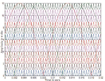
Figure 2. Modulating and carrier waveforms for ISCUPDPWM strategy (ma = 1 and mf = 40 )
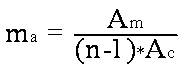
In this strategy, carriers seem to be invert in their phase in turns from previous one so it is named as Alternate Phase Opposition Disposition PWM (APODPWM) strategy. Carrier arrangement for this strategy is shown in Figure 3. Carrier set placed above the zero reference with Amplitude Modulation index for this strategy is defined as:
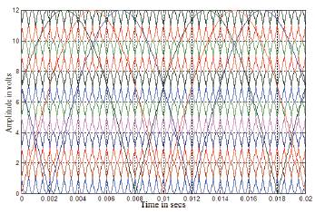
Figure 3. Modulating and carrier waveforms for ISCUAPODPWM strategy(ma = 1 and mf = 40 )
Switching pattern is not equal in PDPWM strategy, so to balance the fluctuations in switching pattern for all the switches, variable frequency PWM scheme is used as illustrated in Figure 4. Here carrier frequency of the intermediate switches is properly increased to balance the number of switching for all the switches. All carriers are in same phase, same amplitude and varying frequency. Hence it is named as Variable Frequency PWM (VFPWM) strategy. Amplitude Modulation Index for this strategy is defined as:
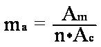
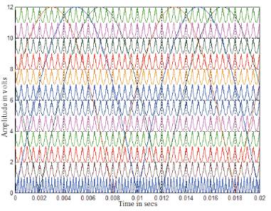
Figure 4. Modulating and carrier waveforms for ISCUVFPWM strategy(ma = 1 and mf = 40 for upper switches and ma = 1 and mf = 80 for intermediate switches)
In this method all carriers have the same frequency, same phase and amplitude of each carrier chosen as 1.6 and overlapping amplitude will be 0.8(Ac/2), where Ac is overlapping amplitude of the carrier. Carrier arrangement for this pattern in shown in Figure 5. Amplitude Modulation for this ISUCOPWM scheme is defined as:
Simulation studies are performed by using MATLAB SIMULINK to verify the proposed PWM strategies for chosen three phase seven level inverter for various values of ma ranging from 0.6–1 and corresponding %THD values are measured using FFT plot and they are shown in Table 1.
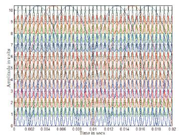
Figure 5. Modulating and carrier waveforms for ISCUCOPWM strategy (ma = 1 and mf = 40 )
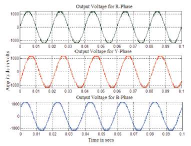
Figure 6. Simulated output voltage generated by ISCUPDPWM technique for R-load
Table 2 shows the VRMS (fundamental) output of inverter for the same modulation indices. Table 3 shows the form factor for different modulation indices which are calculated using RMS voltage and DC component from FFT plots. Table 5 shows crest factor values which are measured using peak voltage and RMS voltage from FFT plots. Table.5 shows the distortion factor for different modulation indices. Figures 6-13 show the simulated output voltages of chosen twenty-five level inverter and the corresponding FFT plots with different strategies but only for one sample value of ma = 0.8 and mf =40. Figure 6 shows the twenty-five level output voltage generated by ISCUPDPWM strategy and its FFT plot is shown in Figure 10. Figure 7 shows the twenty-five level output voltage generated by ISCUAPODPWM strategy and its FFT plot is shown in Figure 11. Figure 8 shows the twenty-five level output voltage generated by ISCUVFPWM strategy and its FFT plot is shown in Figure 11. Figure 9 shows the twenty-five level output voltage generated by ISCUCOPWM strategy and its FFT plot is shown in Figure13. It is recognised from the overall analysis that the lower order harmonics are eliminated as we go for higher number of levels. The following parameters are used for the simulation results Vdc=100V, fc=2000Hz, fm=50Hz and R=100Ω.
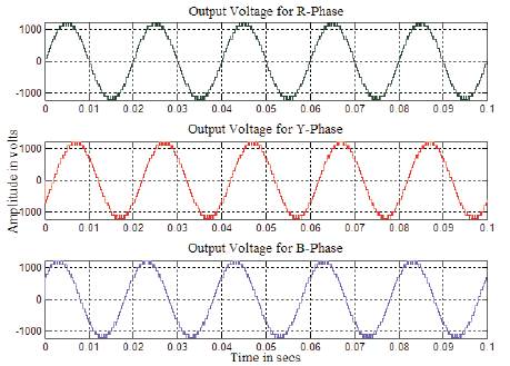
Figure 7. Simulated output voltage generated by ISCUAPODPWM technique for R-load
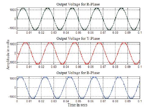
Figure 8. Simulated output voltage generated by ISCUVFPWM technique for R-load
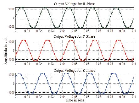
Figure 9. Simulated output voltage generated by ISCUCOPWM technique for R-load
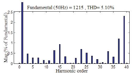
Figure 10. FFT spectrum for ISCUPDPWM technique
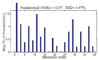
Figure 11. FFT spectrum for ISCUAPODPWM technique
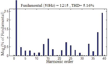
Figure 12. FFT spectrum for ISCUVFPWM technique
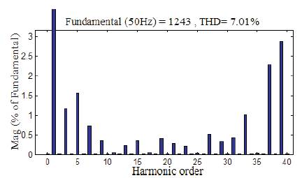
Figure 13. FFT spectrum for ISCUCOPWM technique
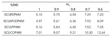
Table 1. % Thd of Output Voltage of Chosen Mli for Various Values of Modulating Indices
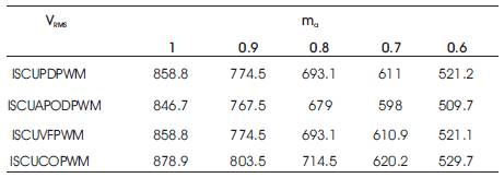
Table 2. Vrms (fundamental) Of Output Voltage Of Chosen Mli For Various Values Of Modulating Indices
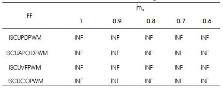
Table 3. Form Factor Of Output Voltage Of Chosen Mli For Various Values Of Modulating Indices
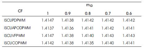
Table 4. Crest Factor Of Output Voltage Of Chosen Mli For Various Values Of Modulating Indices
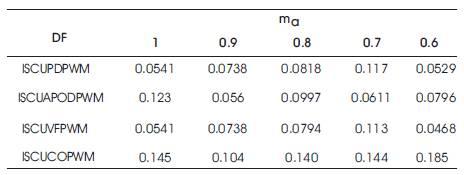
Table 5. Distortion Factor Of Output Voltage Of Chosen Mli For Various Values Of Modulating Indices
In this paper, various new schemes adopting the constant switching frequency and also variable switching frequency multicarrier control freedom degree combination concepts are developed and simulated for the chosen three phase MLI. Performance indices like %THD, VRMS (indicating the amount of DC bus utilization), CF, FF and DF related to power quality issues have been evaluated, presented and analyzed. Tables 1, 2 show the THD and VRMS respectively. Table 3 presents DF for all modulating indices. Tables 4, 5 display CF and DF for all chosen modulating indices. The result analysed indicate that appropriate ISUPWM strategies have to be employed depending on the performance measure required in a particular application of MLI based on the criteria of output voltage quality (Peak value of the fundamental, THD and dominant harmonic components). The proposed topology which is applicable for any number of higher levels with less THD can be implemented in industrial applications such as AC Power Conditioners, Static VAR Compensators, Drive Systems, etc and in power generation industries.