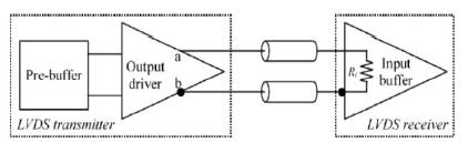
Figure 1. Simplified Schematic of LVDS link
Low Voltage Differential Signaling (LVDS) technology is an effective solution for the physical layer of high-speed data applications. The advantages of the LVDS interface include high data rates, low noise generation, and low power consumption across the entire speed range. Different approaches of LVDS circuit implementation are considered in this article. The LVDS transmitter circuit implementation in the I/O pad cell for microprocessor product based on 65nm CMOS bulk technology is presented. The designed LVDS transmitter supports a 600 Mbps data transfer rate and supply current no more than 5mA.
Low-Voltage Differential Signaling (LVDS) is defined in two separate industry standards: the generic electrical layer standard ANSI/TIA/EIA-644-1995 created by the Telecommunication Industry Association – Electronic Industry Association [1], and the IEEE 1596.3-1996 specific standard that is based on the physical layer defined for the Scalable Coherent Interface (SCI) [2]. LVDS is currently recognized as one of the best point-to-point interfaces suitable for Gbps data rates. The main advantage offered by LVDS is its low voltage swing of 250–450 mV [1], which allows for high-speed interface operation at a very low level of power consumption. In addition, true differential signaling increases the interface's tolerance to ground mismatch between transmitter and receiver. It also improves signal EMI immunity and compliance.
Traditionally, LVDS input–output buffers (I/Os) are used in Complementary Metal-Oxide-Semiconductor (CMOS) Integrated Circuits (ICs) as efficient alternatives to standard single-ended interfaces. These I/Os utilize MOS transistors for their active devices. The advantages of the LVDS interface include high data rates, low noise generation, and low power consumption across the entire speed range. From an economical point of view LVDS can provide cost savings in the following ways: the ability to use inexpensive CMOS technology processes for LVDS chip manufacturing, does not require many voltage sources and complex cooling systems, LVDS transmitters are area efficient and can be integrated in an I/O pad.
The main goal of this paper is to describe architecture choices, circuit implementation, and features of the LVDS transmitter I/O pad. The first part of the paper describes LVDS transmitter architectures. The second part describes the functional diagram of the LVDS transmitter and the circuit implementation of the I/O including block, output driver and common mode control negative feedback and logic control circuits. Simulation results (output waveforms and AC stability) are also presented in the second part of article. The third part of the paper describes the LVDS transmitter features for the microprocessor product and silicon waveform measurements.
In general, an integrated output buffer includes an output driver and pre-buffering circuitry that performs internal signal amplification and conditioning required for correct driver operation. An LVDS output driver is a switch-bridge with two outputs “a” and “b,” which source and sink constant current of reversible polarity into a 100 Ohms differential load typically represented by a termination resistor. A simplified schematic of a point-to-point LVDS link is shown in Figure 1.
Figure 1. Simplified Schematic of LVDS link
The previously mentioned IEEE standard defines limitations on the driver's most important parameters including the output high and low voltages, the output differential voltage swing, the output offset voltage, and impedances of both the direct and inverted outputs in the range from dc to a maximum operational frequency. Some other parameters like currents for the outputs shorted to ground or together are also specified.
For correct operation of the driver, two parameters of the output signal must be stabilized: the output swing and the offset voltage. In addition, the impedances of both singleended outputs must be closely matched. The other output driver parameters are much easier to satisfy and will not be discussed in this section for the sake of simplicity. However, the values of these parameters achieved for the designed output buffer will be presented later on in this paper. Correct LVDS output driver functionality can be achieved through one of three possible architectures [3-5], which are illustrated using their equivalent circuit models in Figure 2.
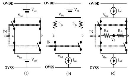
Figure 2. LVDS Output Driver Architectures
Three kinds of architectures are presented: VSVS output driver (Figure 2(a)), VSCS output driver (Figure 2(b)) and CSCS output driver (Figure 2(c)). All solutions have advantages and disadvantages as described in [5]. Also [5] describes VSVS driver as most low-power solutions and shows circuit implementation in bipolar technology basis. However, the VSVS approach requires two stable voltage sources (supposes two negative feedback) which are difficult to implement in CMOS technology due to the large area for compensation capacitors and the need for good device matching. The VSCS approach has both the disadvantages from VSVS and CSCS approaches. The CSCS driver can consume a little bit more current (due to additional current which flows through Rfb resistors) and has only one negative feedback to stable common mode (offset) output voltage. It can be implemented easily in CMOS basis. Therefore, CSCS approach is chosen for I/O LVDS pad implementation for microprocessor product. Please note that this approach requires implementation of voltage reference circuit and current reference circuits.
The CSCS output driver configuration includes both a current source and a current sink as shown in Figure 2(a). Its main downfall is the requirement for exact matching of the source and sink currents and to provide a stable common mode (offset) voltage. The proposed LVDS transmitter block diagram simultaneously provides common mode voltage stability and current sources matching by one negative feedback (Figure 3).
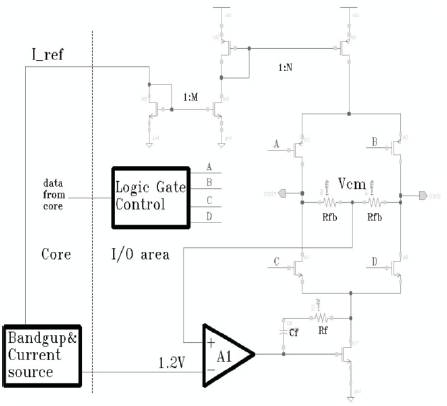
Figure 3. LVDS Transmitter Block Diagram
The diagram contains a bandgap voltage reference providing stable voltage ~1.2V as well as a current reference block providing I/O cell supply current. Also included are current mirrors, an output driver (four switches), a differential amplifier placed in negative feedback operation mode, and a logic gate control block. The operation is as follows: The bandgap voltage reference provides a stable 1.2V voltage. This voltage is applied to the positive input of the differential amplifier. The current reference circuit provides a reference current to the current mirrors. The current mirrors supply all internal blocks of I/O and provide the output driver current. The output driver contains internal resistors Rfb. A portion of the driver's current flows through the Rfb resistors and provides Vcm internal voltage offset. The Vcm internal voltage offset comes to the negative input of the differential amplifier. The differential amplifier compares both voltages on positive and negative inputs and drives transistors so that Vcm voltage is equal to the 1.2V reference voltage. Also the sink current is equal to the source current on this diagram. The logic gate control block drives transistors A,B,C and D in opposite phases to provide a differential signal between padn and padp points.
Figure 4 shows the part of LVDS segment and supply block which provide reference voltages and currents. Bandgap reference and current reference circuits are common for LVDS I/O cells in each segment and located in the middle of segment in core area. Therefore 1.2V bus and current buses have to be routed to all LVDS I/O cells and the current reference circuit has to include current sources equal to the number of LVDS I/O cells.
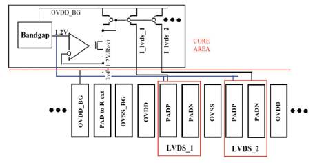
Figure 4. Part of LVDS Segment and Supply Block
Bandgap Voltage reference circuit design is provided based on [6]. The current reference circuit is implemented based on negative feedback property and external resistor usage to get stable current value in all technology processes.
Figure 5. presents the output driver schematic (Figure 5(a)) and schematic of the analog part (Figure 5(b)) of the LVDS I/O cell which allow to stabilize current and common mode voltage value.
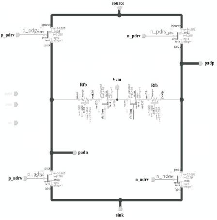
Figure 5(a). Output Driver Circuit
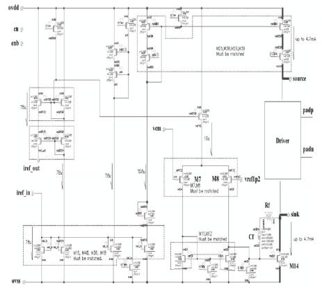
Figure 5(b). Analog Part of LVDC I/O cell
When voltages on differential amplifier inputs (M7 and M8) differ, the differential amplifier drives transistor M14 to reduce this difference because the drain current of transistor M14 is stable. This negative feedback system requires frequency compensation due to the possibility of oscillation. A capacitor with serial resistor (Rf and Cf) is used between drain and gate of M14 to provide frequency compensation and achieve a phase margin no less than 70 degree to avoid oscillations. Simulation results of frequency analysis are presented on Figure 6.
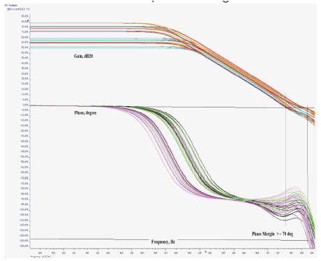
Figure 6. LVDS feedback AC analysis simulation results for all process, temperature and supply voltage combinations
Logic gate control provides four signal switches from input digital signal to drive four output switches. To provide correct common mode feedback operation, the logic gate control block disallows the situation when all switches are turned off simultaneously. The following conditions have to be provided to avoid this condition (Fig. 7) :

Also p_pdrv and p_ndrv signals should be separate in time to reduce short circuit current, but it is not necessary.
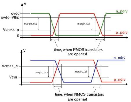
Figure 7. Logic control output signals
Simple simulations show how simultaneous turning all output switches off impacts the common mode voltage stability (Figure 8(a) and Figure 8(b)).
The LVDS I/O cell logic gate control block schematic implementation contains a hysteresis system which allows avoiding simultaneously turning output switches off. Simulations are provided for all processes, temperatures and supplies combinations. It shows that results correspond to situation on Figure.8(b).
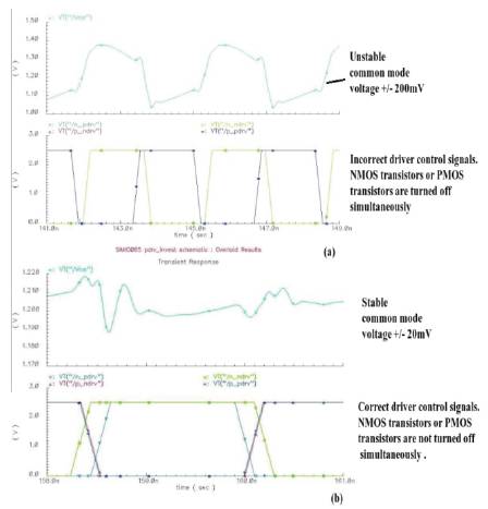
Figure 8. Common mode voltage stability vs. control signal timing effect. (a) unstable, (b) stable
Tables 1-3 show DC operational conditions, and DC and AC parameters provided by the LVDS I/O. The output current is placed in range from 2.5mA to 4.5mA, and the amplitude of differential output signal ranges from 250mV to 450mV. The common mode voltage ranges from 1.075V to 1.325V. The typical operating frequency of the LVDS I/O transmitter is 300MHz. AC parameters are simulated with several LVDS schematics in one segment and with parasitic bus inductance and capacitors elements to take into account SSN effects. Transition low and transition high time is in ranges from 0.26ns to 0.5ns. Common mode voltage (offset) imbalance is no higher than 150mV.
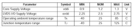
Table 1. LVDS DC operating conditions
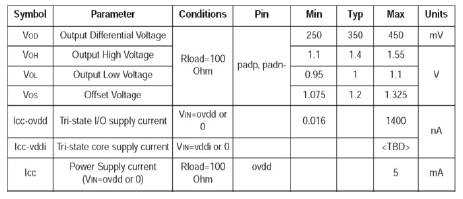
Table 2. LVDS I/O DC parameters
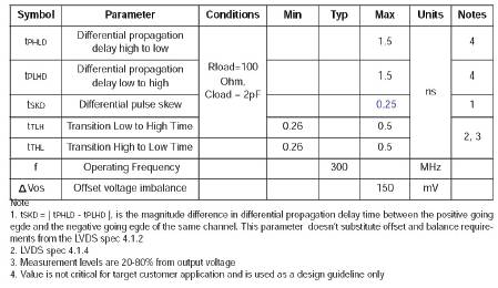
Table 3. LVDS I/O AC Parameters
The LVDS I/O transmitter architecture has sufficient margin beyond its typical operating frequency of 300MHz. Output differential signal and common mode voltage simulation waveforms at 500MHz operation frequency are presented in Figure 9.
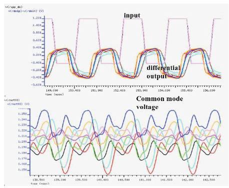
Figure 9. Output differential signal and common mode voltage simulation Waveforms at 500MHz
The LVDS I/O transmitter on the microprocessor product has several features. The LVDS cell meets the JTAG standard and contains a BSR block and two CMOS inputs on positive and negative paths. The LVDS segment supply architecture provides external instead of internal resistors to reduce output current deviation. When the system uses the internal resistor option, BG_res pad can be used as the input LVDS signal for functional testing.
The LVDS I/O pad is designed in a 65nm seven-layer metal CMOS bulk process as part of multimedia processor. The layout view of LVDS is presented in Figure 11(a). Figure 11(b) shows the eye diagram of the LVDS transmitter output differential signal measured on silicon received in Q1'2010.
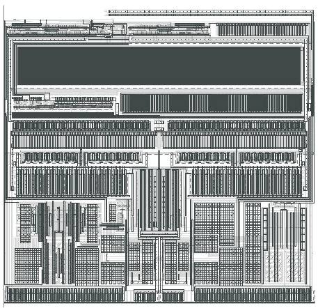
Figure 11(a). LVDS I/O Layout view
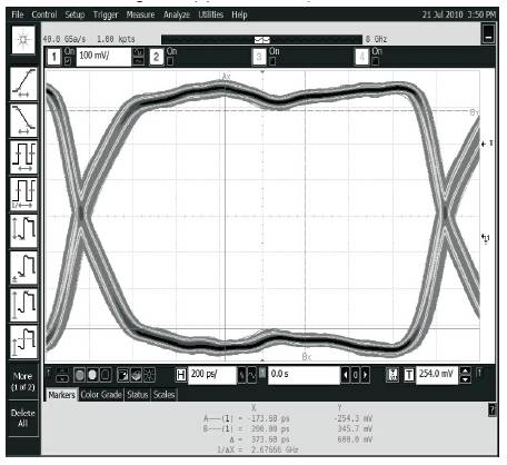
Figure 11(b). Eye Diagram
In multimedia processor, a segment of LVDS I/O pads provides transfer video information to the flat panel with 300MHz operating frequency. This corresponds to a 600 Mbps data rate. The designed LVDS transmitter supports data transfer at 600 Mbps at a supply current no more than 5mA per I/O cell.