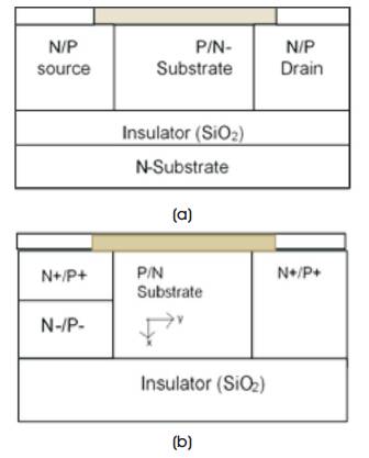
Figure 1 (a) Conventional FD-SOI MOSFET, (b) Modified Source n/p FD SOI MOSFET
The Fully Depleted Silicon-On-Insulator (FD SOI) MOSFETs have been already proved as a favorable CMOS technology node beyond 100 nm and the concept of source modification has been adopted in order to improve the electrical controllability of the device. The one of the major challenges in the design of FD SOI MOS device is the appropriate selection of front and back oxide (BOX) thickness. As the selection of front oxide, with proper thickness and material, is a pathway to avoid off-state gate tunneling to conquer various off-state leakages. While, the buried oxide (BOX) layer is dominant to overcome short channel effects and to reduce drain electric field penetration towards the SOI/BOX interface. This paper demonstrates the impact of front and back oxide (BOX) thickness variations on performance of modified source FD SOI MOSFET at 50 nm gate length. The impact of front and back oxide (BOX) thickness variations have been analytically evaluated by using twodimensional surface potential and drain current model, and verified against the simulated results. It has been verified that the device exhibits more uniform electric field in the channel. That assures low off-state leakage current and reduced short channel effects in the device. The Ion to Ioff ratio of the device is found to be 1010 and hence the device is suitable for low power digital applications. The device has also been designed and simulated using TCAD device simulator.
Digital devices are progressive across the globe today by making communication and sharing easier than ever. At the console of each digital device, semiconductor chips are present that enhance power and intelligence to control the device. Each semiconductor chip is made of millions of transistors. In order to construct better digital world and improve the quality of the device and user experience, the scaling of the transistors has been continuously done while increasing per formance and reducing power consumption. However, due to scaling of transistor’s, the length of the channel is reduced and controllability of gate over the channel also reduces [1]. This will cause various Short-Channel Effects (SCEs) and off-state leakage in the device that degrades the device performance. With innovative technology nodes to enhance performance and turn down the adverse SCEs to improve the device reliability, It has been the main focus in today's MOSFET nano era. The various issues linked with available nano MOS technology nodes are the Drain Induced Barrier Lowering (DIBL), parasitic capacitances, threshold voltage (Vth ) variability and off-state leakage [2].
Silicon-On-Insulator (SOI) technology substrates made possible to enhance the device performance by reducing off-state leakage with increased drive current and also lowered parasitic capacitances effects [3]. The two types of SOI substrates have been discussed in literatures PD-SOI and FD-SOI. In the present research works, for low power devices, FD SOI MOSFETs are mainly used. FD-SOI MOSFET is a nano CMOS technology, especially designed to serve at low power while enhancing performance, manufacturability and lowest cost [4]-[11]. FD SOI technology offers reduced dopant fluctuations, lower Vth roll off, good electrostatic control, reduced power consumption, and low leakage. Hence, short channel effects are reduced due to low leakages. However, the electric field penetration from drain region to the SOI/BOX interface through BOX layer must be reduced in order to suppress the short channel effects and enhance the performance, which can be solved by choosing buried oxide layer of convenient thickness and material [4]. There are various ways to reduce the short channel effect at SOI/BOX interface, such as Improving the BOX layer, SOI layer, and the substrate layer.
Mishra, and Chauhan have discussed the performance analysis of CMOS inverter circuit based on fully depleted ultrathin- body MOSFET for low power digital applications [5]. For the modelling of various devices the different analytical models have been proposed [6]-[9]. Surface potential based MOSFET models provide authentic expressions for potential along the channel, threshold voltage, and inversion charges. Surface potential modeling is also adopted to see the electric field variation in the device. Young had developed a model by taking a 2nd order analytics for the potential variation vertical to the channel and found a 2-D potential distribution in the layer of SOI [6]. However, the model does not depend upon back oxide thickness as Young had assumed that electric field at the bottom of the SOI layer was zero. In order to dictate the aspects of back oxide thickness, Suzuki, and Pidin discussed a model for threshold voltage of FD-SOI MOSFETs, by assuming 2-D variations in SOI and insulator layer and concluded that, sometimes back oxide (BOX) layer may affect the performance of the device, yet insulator layer had very less dependency, depending upon the parameter under consideration [7]. Kumar and Chaudhry had developed a model for the surface potential forward to the device channel in FD-SOI MOSFETs [8]. The device has gained popularity due to its dual material gate performance. Karatsori, et al. had developed a drain current compact model for lightly doped short-channel Ultra-Thin Body Box (UTBB) FD SOI MOSFET and described DIBL, channel length modulation effects with the back-gate control dependency on the drain current [9] . Mishra and Chauhan have recently proposed a device, in which a new concept of two levels of source doping has been utilized in the design of modified source FD SOI MOSFET [10]. The electrical performance of the device was discussed on the basis of simulation results. It has been reported that the device exhibits low off-leakage and high Ion /Ioff ratio, which is quite high as compared to other available MOS devices at this technology node. So, it is therefore necessary to verify these objectives and its electrical characteristics by device modelling.
In this paper, analytical model (surface potential and drain current model) has been studied for performance verification of modified source FD SOI MOSFET [10] and the impact of front and back oxide thickness has been seen at 50 nm gate length. The design of the studied structure is also easy to fabricate as compared to other available MOS technology such as MugFET, FinFET, and TFET. Since, this device has high Ion /Ioff ratio and low threshold voltage, it is suitable for low power digital applications.
The conventional FD SOI MOSFET structure has been shown in Figure1(a). Figure 1(b) shows the studied structure of modified source FD-SOI n/p-MOSFET at 50 nm gate length. In modified source FD-SOI n-MOSFET, lightly doped N- is introduced below the N+ source region and viceversa for p-MOSFET. The fabrication of this device is also simple and this is very similar to TDBC SOI n-MOSFET [11].
Figure 1 (a) Conventional FD-SOI MOSFET, (b) Modified Source n/p FD SOI MOSFET
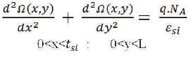
Table 1 shows the various device parameters and specifications of the studied structure modified source FD-SOI MOSFET [10]. In Table 1, the front and back oxide (BOX) thickness is made variable to decide the optimized dimensions. The gate to source voltage used for modelling is taken as 1.1 V
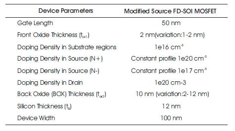
Table 1. Device Parameters of Modified Source FD SOI N-MOSFET
In Modified Source FD-SOI n-MOSFET, two different levels of source doping have been considered in the source region, so that a low doping N- profile is placed under the N+ source profile region which is different from a placement of P+ profile under the N+ source region of Tunnel diode body contact SOI n-MOSFET [11]. This is done in order to get low parasitic capacitance and improved electric field in the channel.
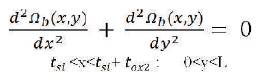
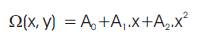
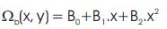
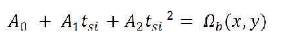
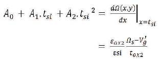
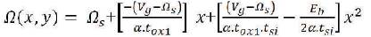
The schematic cross-sectional view of the modified source FD-SOI MOSFET is shown in Figure 1 (b). According to Poissons' equation, the two-dimensional potential distribution in the channel area and in BOX region are given by,
where NA is the doping profile in the silicon film, ε
The solution of equations (1) and (2) can be targeted as second order polynomial equation for the solution,
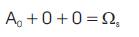
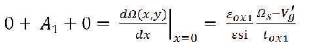
By using boundary conditions [6] for equation (3) in which potential is assumed to be continuous at silicon surface and by approaching for solution [7],
Now the obtained solution can be written as
and by putting x = tsi , the solution of potential in buried oxide region [7]
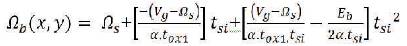
where tox1 and tox2 are front channel and back channel (BOX) thickness, respectively. εox1 and εox2 are front and back channel oxide permittivity constants, respectively and Eb is the electric field profile in BOX and α = εsi/εox
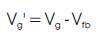
where, Vg is the applied gate voltage and
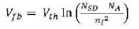
where Vfb is the flat band voltage and is given by
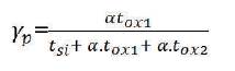
In this paper, the authors have introduced two process parameters such as
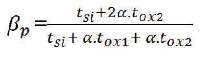
and
where,Ωs = (x, y) at x=0 and by substituting the process parameters from equations (6) and (7),Ωs can be written as,
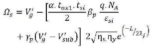
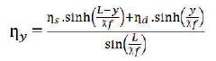
where, Vth is the thermal voltage, NSD is the uniformly doped source/drain concentration and ηs,ηy ,λf are device parameters and the device parameters ηs and ηy’ can be defined as [7],
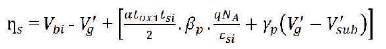
where ηD= ηs +VDS and Vbi is the built-in potential. In modified source FD SOI MOSFET, Vbi will vary according to the levels of the source doping. By substituting the expression of ηs and ηy from equations (16) and (17) in equation (15) for Ωs and hence substitute in equations (9) for Ω(x,y)
All surface potential based compact models use charge sheet approximation to get drain current of the device. By using drift diffusion model, the drain current (Id ) can be approximated as [9],
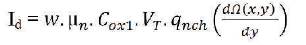
where w,μn , Cox1 , VT are the device width, mobility, front oxide capacitance at thermal voltage, and qnch is the normalized charge in the channel [9]. By differentiating the surface potential from equation (9), the drain current modeling can be achieved and same results have been discussed in the result and discussion section.
The modified source FD SOI MOSFET is shown in Figure 1 (b) and the device parameters used for calculation are shown in Table 1 with gate to source voltage (Vgs ) of 1.1 V. Figure 2 shows the variation of surface potential along the channel. Figure 2 (a) shows the surface potential variation along the channel with varying thickness of N+ layer in source region from 5 to 2nm, obtained from the model. It has been found that, as the N+ layer thickness varies from 5 to 2 nm, the position of minimum surface potential near to the source region is maintained at around 20 nm. This clearly indicates that the weak inversion is occurring at the source side of the channel and that assures almost negligible off-state leakage in the device at N+ layer thickness of 2 nm in the source region. Hence the N+ layer thickness of 2 nm has been taken by default for further results analysis.
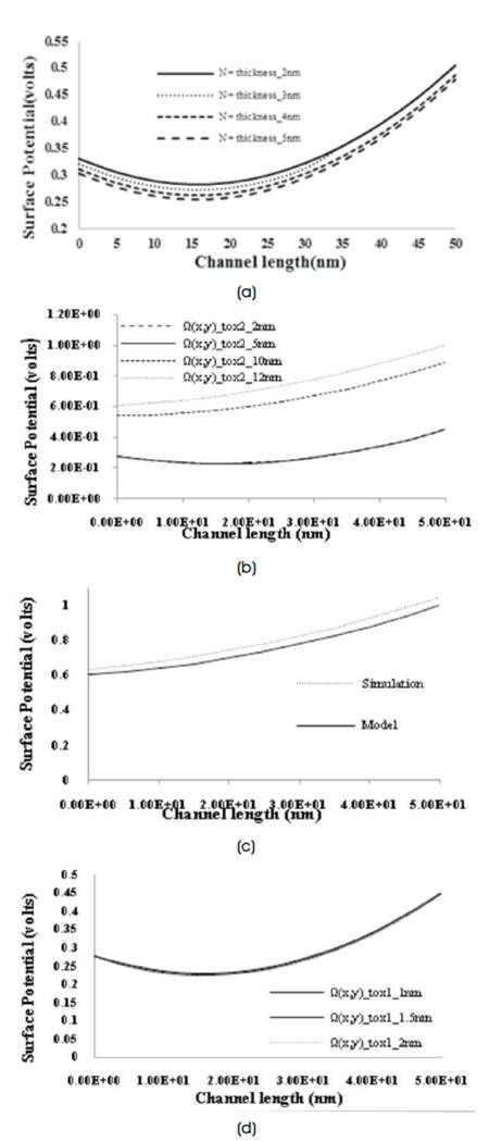
Figure 2. Surface Potential Model (a) Surface Potential Variation as a Function of Channel Length for Modified Source FD SOI MOSFET with varying Thickness of N+ Layer in Source Region, (b) Surface Potential along the Channel at back Oxide at varied Back Oxide Thickness (tox2 ) obtained from Model, (c) The Comparison of Surface Potential obtained from Model and Simulation at an Optimized Back Oxide Thickness of 10 nm, (d) Surface Potential Variation along the Channel at Different Front Oxide Thickness (tox1 )
Figure 2 (b) shows the variation of surface potential along the channel at different back oxide thickness (tox2 ) obtained from model. One can see from the result, as the back oxide thickness is changed from 2 to 12 nm, the minima position of surface potential is moving towards the source side of the channel. This will lead to more uniform electric field in the channel which clearly indicates that the gate controllability is enhanced and due to this, the short channel effects will be reduced. Hence the drive current will increase and reduce the offstate leakage. The main region behind this improvement is due the reduction in drain electric field penetration. Moreover, this is also due to compressive stress provided by the BOX insulator. As the BOX thickness is increased, the induced compressive stress reduces and the positive impact takes place. So, the results inferred that the optimized thickness of the back oxide is 10 nm.
Figure 2 (c) shows the comparison of surface potential obtained from model and simulation at an optimized back oxide thickness of 10 nm. There is a negligible deviation seen in simulation and model results. Figure 2 (d) shows the surface potential variation along the channel at different front oxide thickness (tox1 ) dielectric and back oxide (BOX) thickness of 10 nm. Also, the high gate dielectric material HfO2 has been used to avoid off-state tunnelling. As the front oxide thickness is varying from 1 to 2 nm, the weak inversion region is maintained near source region with a minima position of 15 nm. However, as the tox1 increases from 1 to 2 nm, the quantum mechanical tunnelling will be reduced before the onset. This will solve the leakage issues in the device.
Figure 3 shows the input characteristics of modified source FD SOI MOSFET at Vgs = 1.1 V. Figure 3 (a) shows the input characteristics at different back oxide thickness (tox2 ) obtained from the model. It can be inferred that as the back-oxide thickness is increased from 2 to 12 nm, the offstate current of the studied structure is also decreased, while the drive current is almost the same. This reduction in off-state leakage is due to the reduced compressive stress and potential effects as discussed in surface potential model result section. The Ioff current obtained from the model is 42.7 pA and Ion current as 2 mA at 50 nm channel length at an optimized thickness of 2 nm and 10 nm of front and back oxide, respectively. The ratio of Ion /Ioff is 1010 . The structure shows a subthreshold slope of 58 mV/decade at room temperature. Figure 3 (b) shows the comparison of Id vs. Vgs characteristics obtained from model and simulation. There is minor deviation seen in the plots. Figure 3 (c) shows the Id vs. Vgs characteristics obtained from model for varying thickness of front oxide thickness from 1-2 nm at an optimized back oxide thickness of 10 nm. It can be concluded from the graph, as the front oxide thickness is increasing, the off-state leakage current is getting reduced. This is also due the reduced quantum mechanical tunnelling effect during off-state and hence threshold voltage roll off is not taking place. As per ITRS roadmap, as the thickness of the front oxide decreases, the metal gate material and work function plays an efficient role in designing of nano MOS devices. Here gate metal of work function 4.2 eV has been used.
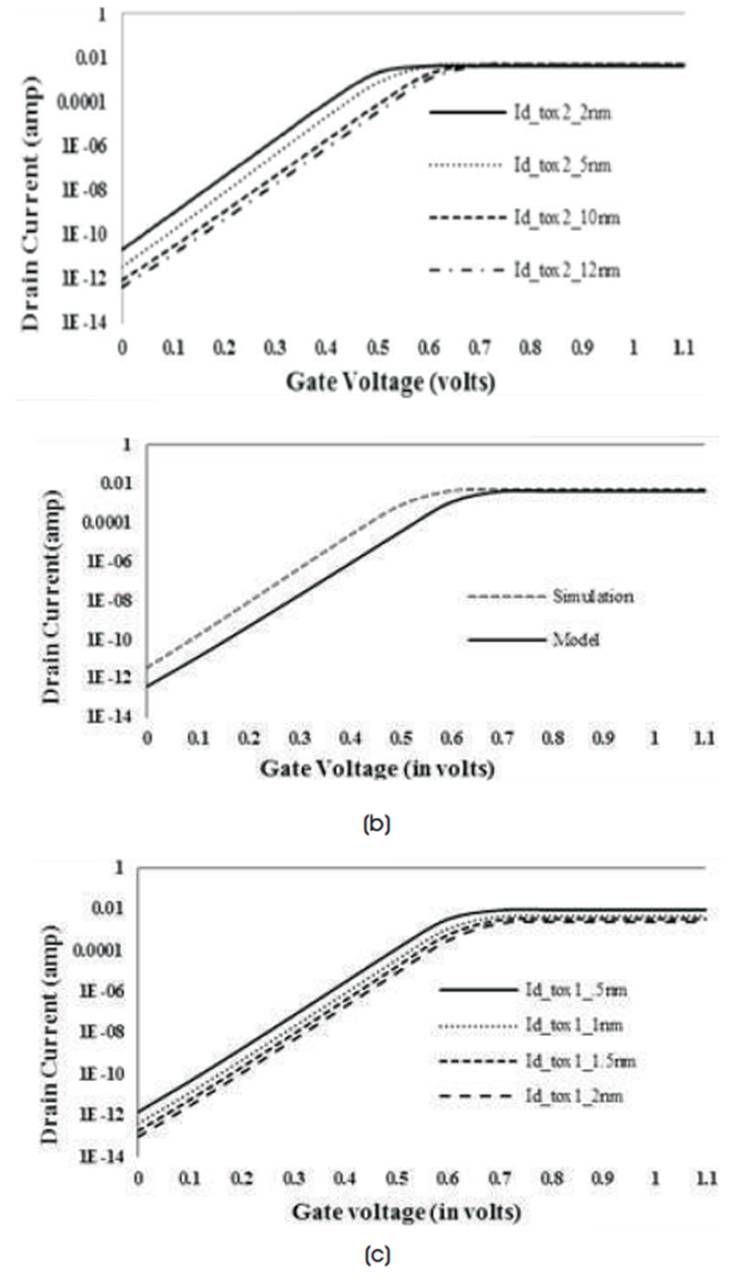
Figure 3. Drain Current Model (a) Input characteristics curve (Id vs. Vgs) at different Back Oxide Thickness (tox2 ) obtained from model (b) Comparison of Id vs. Vgs Characteristics obtained from model and simulation, (c) Id vs. Vgs characteristics obtained from model for varying thickness of Front Oxide Thickness from 5-2 nm at an optimized Back Oxide Thickness of 10 nm
From the above analysis, it is clear that the device is showing high drive current and very low off-state leakage current at an optimized thickness of front and back gate oxides. As, there is a requirement of high drive current in order to get high fan out of any digital circuit and the offstate leakage assures the very low power dissipation. So, the device under consideration can be the best alternative for a digital circuit design.
In this work, the impact of front and back oxide thickness variation on electrical performance of modified source FD-SOI n-MOSFET has been evaluated by studying 2-D surface potential variation along the channel and by current-voltage model. The device has also been designed and simulated using TCAD device simulator. It has been found that the device is showing better immunity towards the short channel effects and the device is showing lower off-state leakage current (Ioff ) of 42.7 pA at an optimized front and back oxide thickness (BOX) of 2 nm and 10 nm, respectively. The Ion to Ioff ratio of the device is found to be 1010 and there is also scope of improved switching by using high gate materials even at front oxide thickness of 1 nm. The prime apprehension behind the per formance enhancement is the competency of modified source FD SOI MOSFET towards the suppression of drain electric field penetration at SOI/BOX interface. Hence, modified source concept in FD SOI MOSFET solves the various challenges associated with the current MOS technologies and such short channel effects, overcome the problem of Random Dopant Fluctuations (RDFs) as no use of highly doped substrates, reduced off-state leakage and less power consumption requirement's. The studied structure is compatible with the CMOS inverter circuit and other digital circuits.