Figure 1. Schematic of Conventional Full Adder
This paper proposes a 1-bit Full adder using Fin type Field Effect Transistor (FinFET) at 250 nm CMOS technology. The paper is intended to reduce leakage current and leakage power, chip area, Delay and to increase the switching speed of 1-bit Full Adder while maintaining the competitive performance with few transistors used. In this paper, first part implemented Standard CMOS full adder that uses 28 transistors and the next part deals with the implantation a Double-Gate (DG) FinFETs based full adder, which uses 10 transistor count with suitable power consumption, delay performance. and the next part extracting their transfer characteristics by using Synopsys TANNER-EDA simulation tool. The authors investigate the use of Double Gate FinFET technology, which provides low leakage and high-performance operation by utilizing high speed and low threshold voltage transistors for logic cells. It shows that it is particularly effective in subthreshold circuits and can eliminate performance variations with Low power. A 22 ns access time and frequency 0.045 GHz provide 250 nm CMOS process technology with 5 V power supply is employed to carry out 1-bit Full Adder of speed, power, and reliability compared to MOSFET based full adder designs. Hence FinFET is a promising candidate and is a better replacement for MOSFET.
In today's trend, any portable electronic devices like Laptops, Mobiles, etc., should be smaller and smarter. Smaller device context in terms of cost and area, smarter device means, it should respond fast, there is an escalating number of portable applications with a limited amount of power available, requiring small area, lowpower, and high throughput circuitry. Therefore, circuits which consume low power become the major concern factor for the design of microprocessors and system components. The research effort in low power microelectronics has been intensified and low power VLSI systems have emerged as exceedingly in demand. The working principle is same as that of planner MOSFET. The conventional bulk MOSFETs suffer from short channel effects at lower technology nodes due to the fact that as the source and drain regions are brought closer together, the drain region is better able to control the carriers in the channel than the gate.
Adder is one of the most important components of a central processing unit, Arithmetic Logic Unit (ALU), and floating point unit and address generation like cache or memory access unit. Low-power and high-speed adder cells are used in battery-operation based devices. As a result, the design of a high-performance full-adder is very useful and vital (Saraswat, Akashe, & Babu, 2013). One of the most well known full adders is the standard CMOS full adder that uses 28 transistors as shown in Figure 1.
Figure 1. Schematic of Conventional Full Adder
In this paper, the authors present a 1-bit full-adder circuit, which uses 10 transistors with suitable power consumption and delay performance. The basic advantage of 10 transistors full adders are-low area compared to higher gate count full adders, lower power consumption, and lower operating voltage (Yadav & Dantre, 2015; Rabaey, Chandrakasan, & Nikolic, 2002). It becomes more and more difficult and even outmoded to keep full voltage move backward and forward operation as the designs with fewer transistor count and lower power consumption are pursued. The basic disadvantage of the 10 transistors full adders are suffering from the threshold-voltage loss of the pass transistors. They all have double threshold losses in full adder output terminals. These drawbacks were overcome in this paper by applying Double gate FINFET technique to 10 Transistor 1-Bit full adder design (Saraswat et al., 2013).
Double Gate FINFET has two electrically independent gates, which gives the circuit designer more flexibility in design (Saraswat et al., 2013). The power consumed for any given function in CMOS circuit must be reduced for either of the two different reasons: One of these reasons is to reduce heat dissipation in order to allow a large density of functions to be incorporated on an IC chip. Any amount of power dissipation is worthwhile as long as it doesn't degrade the overall circuit performance. The other reason is to save energy in battery operated instruments same as electronic watches, where the average power is in microwatts (Junming, Yan, Zhenghui, & Ling, 2001; Bajpai, Mittal, Rana, & Aneja, 2017).
The addition is the most basic arithmetic operation and usually used in any digital electronic devices and Arithmetic Logic Unit (ALU) to add any value of numbers. The commonly used adder cell is full adder, where three inputs, i.e. A, B, and Cin will be added together to calculate the output of Sum and Cout (Chin, Lim, & Tan, 2015). The out expression for Sum and Cout is given by:


where the above equations are generated from the truth table of 1-bit full adder as shown in Table 1.
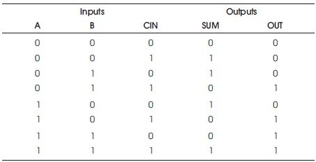
Table 1. Truth Table of 1-Bit Full Adder
The number of research papers of many conferences and journals were studied and survey of the presenting literatures in the proposed work is reported below:
In a parallel transistor, there are two transistors with their source and drain terminals tied together. FinFETs were first introduced by Profs. Chenming Hu, Tsu-Jae King-Liu and Jeffrey Bokor at the University of California in 1999. Most chipmakers are currently developing technologies based on FinFET. These include IBM, Intel, TSMC, Global Foundries, SMIC, Qualcomm AMD, and Motorola. FinFETs are 3D structures that rise above the substrate and resemble a fin. The 'fins' form the source and drain, effectively and in this way, they enable more volume than a traditional planar transistor for the same area. The gate wraps around the fin, and this gives more control of the channel as there is sufficient length for the control. Also as the channel has been extended, there is very little current to leak through the body when the device is in the 'off' state. This also allows the use of lower threshold voltages and it results in better performance and lower power dissipation. The gate orientation is at right angles to the vertical fin. And to traverse from one side of the fin to the other it wraps over the fin, enabling it to interface with three sides of the fin or channel.
FinFET (Figures 2 and 3) is nonplanar double gate transistor built on Silicon on Insulator (SOI) substrate. The important characteristics of the FinFET are that the conducting channel is enfolding by the thin silicon fin, which creates the gate device. The effective channel length of the device is determined by the thickness of the fin. It is called FinFET because the thin channel region stands vertically similar to the fin of a sandwich between the source and the drain regions. The gate covers around the body from three sides and therefore reduces the Short Channel Effect (SCE). A parallel transistor pair consists of two transistors with their source and drain terminals tied together. The second gate is added opposite to the traditional gate. Due to problems in aligning the front and back gates, as well as in buildings a low resistance to the back gate, DGFETs are difficult to fabricate.
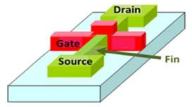
Figure 2. FinFET Structure
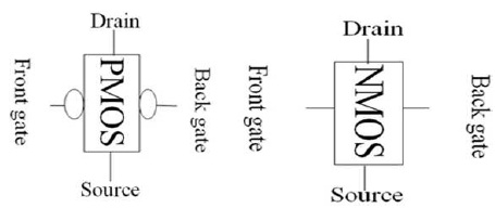
Figure 3. FinFET Symbol
The FinFET has been developed to overcome the problem faced by DGFET. Double gates for FinFETs provide effective control of the short channel effects. It can also be exploited to reduce the number of transistors for implementing logic functions (Palinje, 2018).
Complementary MOS logic style is a combination of two networks; the Pull-up Network (PUN) and the Pull-down Network (PDN). The Pull-up Network consists of PMOS transistors and Pull down Network consists of NMOS devices. The function of Pull up Network is to provide a connection between gate output and Vdd, anytime the output of the gate is meant to be high. Similarly, the function of Pull down Network is to provide a connection between gate output and GND anytime the output of the gate is meant to be low. The Pull-up Network and Pull down Network are mutually exclusive to each other. The noise margin and propagation delay depend on the input patterns.
The existing literature in the proposed area have major challenges that need to be addressed. Some of problems identified are:
The main objective of the research work is to overcome the above mentioned problems and to implement the 1- Bit Full adder using FINFET Technique using Tanner 16.0 Tool in 270 nm CMOS Technology, which will have comparatively less power consumption as compared with the CMOS at 5 V supply.
The CMOS full adder has 28 transistors in the design and it is the simplest implementation based on the above equations. The circuit of CMOS 1-bit full adder is as shown in Figure 4. This design has its advantages and disadvantages. The advantages include high noise margin is very reliable to low voltage. However, a high number of transistors may result in large power consumption, high input loads, and requires larger Silicon area in a wafer. It also stated that this design may introduce more delay because Sum is generated from Cout as input as can be observed from Figure 5 and Figure 6.
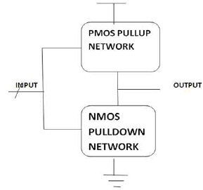
Figure 4. CMOS Logic Style
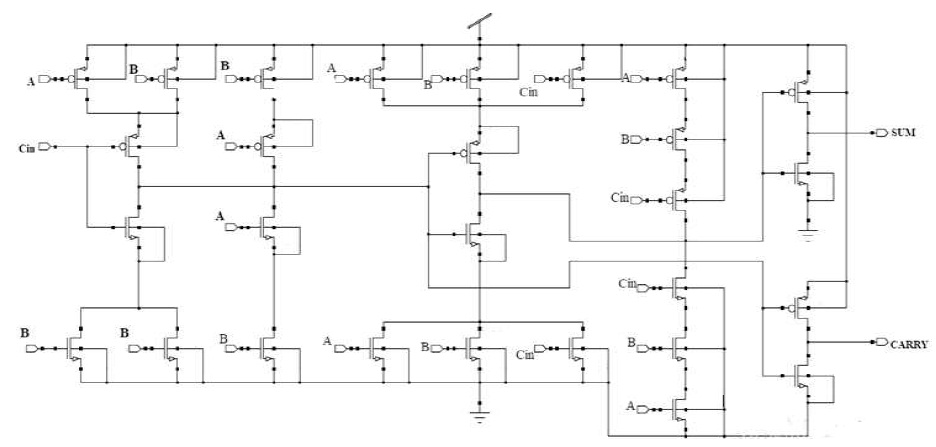
Figure 5. Schematic Diagram CMOS Full Adder
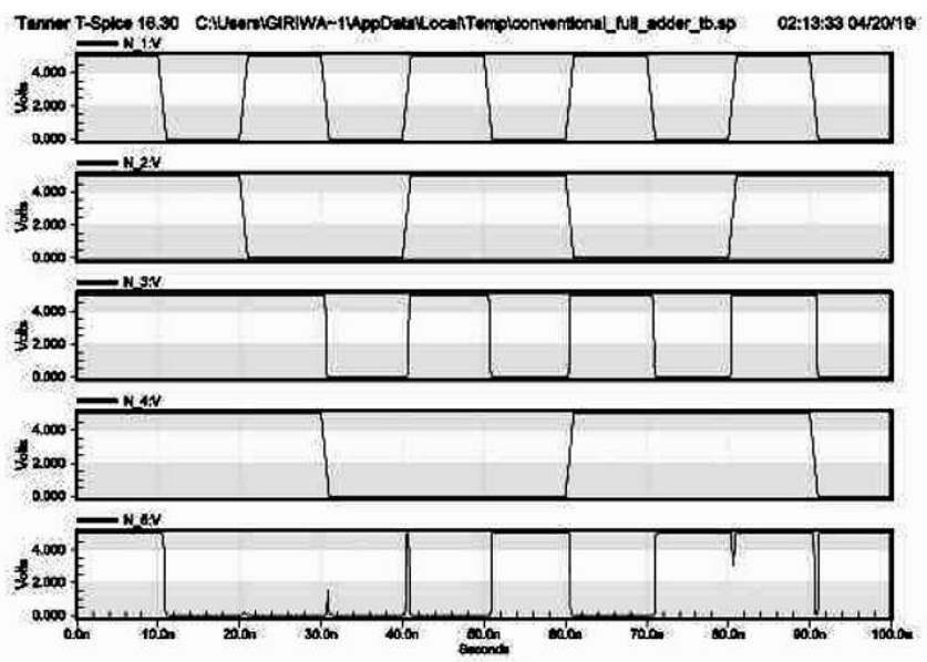
Figure 6. Simulation Result of CMOS Full Adder
Figure 5 shows a symmetric design which is called as CMOS-Bridge. This design generated Carry and Sum with 20 transistors, here using two inverters for improving the driving capability and produce Carry and Sum. The design uses 28 transistors. The output waveforms are following the truth Table 1 of a full adder.
Figure 6 shows the proposed symmetric design and implementation of Double-Gate Circuit with shorted gate mode, which is called as FinFET Bridge. Full adder is a logical circuit with the three inputs (A, B and Cin) and two outputs that are called Sum and Carry. Full adder is one of the core for the arithmetic processors, therefore by increasing the performance of full adder thereby the performance of processors is also increased. The improvement in performance thereby decreases propagation delay. This design generates Cout and Sum with 20 transistors, the use of two inverters is to improve the driving capability and produce Carry and Sum. Here also the design uses 28 transistors.
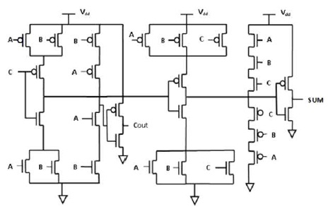
Double gate FINFET technique is applied on 1-Bit Full Adder cell. Here self-determining control of the front and back gate in Double-Gate (DG) can be efficiently used to develop performance and reduce power consumption. In non-critical paths, self-determining gate control can be used to join together parallel transistors. A parallel transistor pair consists of two transistors with their source and drain terminals tied together. The second gate is added opposite to the conventional gate in Double-Gate (DG) FINFETS, which has been predictable for their perspective to superior control short channel effects as well as to control leakage current. The operations of FINFET is recognized as Short Gate (SG) mode with transistor gates attached together, the Independent Gate (IG) mode, where self-determining digital signals are used to drive the two device gates, the low power and optimum power mode where the back gate is attached to a reverse-bias voltage to reduce leakage power, and the hybrid mode, which employs an arrangement of low power and self-determining gate modes. In due to its base material, the uninterrupted down in scaling of bulk CMOS creates key issues. The crucial obstacles to the scaling of bulk CMOS to 250 nm gate lengths include short channel effects, optimum current, gate-dielectric leakage, and device to device variations. But FINFET based designs offer the superior control over short channel effects, low leakage, and better yield in 250 nm helps to overcome the obstacles in scaling The schematic of DG FINFET applied on 1-Bit Full Adder is shown in Figure 7.
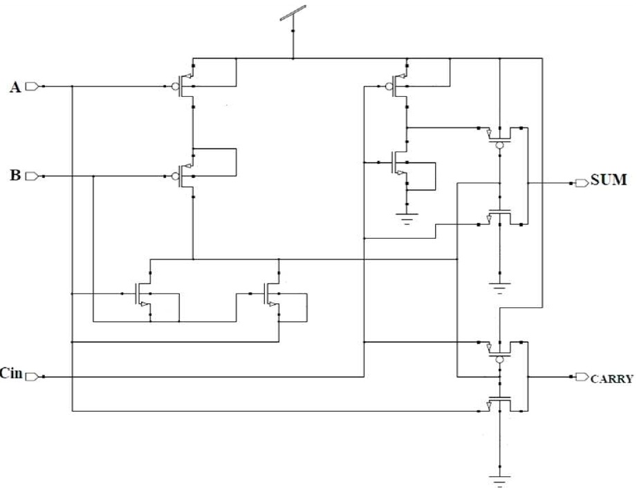
Figure 7. 1-Bit Full Adder using DG FinFET
The output waveform of 1-Bit Full Adder using DG FinFET technique is shown in Figure 8. Digital CMOS circuit may have three major sources of power dissipation, namely dynamic, short, and leakage power. Hence the total power consumed by every Adder can be evaluated using the following equation:
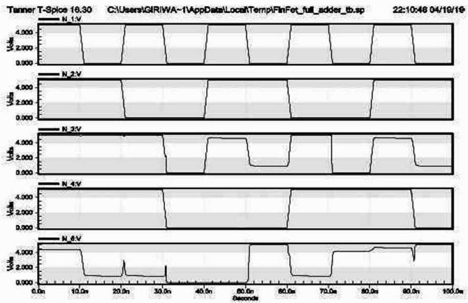
Figure 8. Simulation Result of 1-Bit Full Adder using DG FinFET
Thus for low-power design, the important task is to minimize CLVddVfclk while retaining the required functionality. The first term Pdyn represents the switching component of power, the next component PSC is the short circuit power, and Pleak is the leakage power. Whereas CL is the loading capacitance, Vfclk is the clock frequency which is actually the probability of logic 0 to 1 transition occurs (the activity factor). V is the supply voltage, Vdd is the output voltage swing which is equal to Vdd but, in some logic circuits, the voltage swing on some internal nodes may be slightly less.
The current ISC in the second term is due to the direct path short circuit current, which arises when both the NMOS and PMOS transistors are simultaneously active, conducting current directly from supply to ground. Finally, leakage current Ileak, which can arise from substrate injection and sub-threshold effects, is primarily determined by fabrication technology considerations.
A 1-Bit Full Adder based on DG FinFET technique has been proposed. The analysis of the simulated results confirms the feasibility of the DG FinFET technique in full adder design and shows that there is a reduction of 25 to 30 percent in the value of power dissipation parameter as compared to CMOS technique at a supply voltage of 5 V. DG FinFET adders have a marginal increase in area compared to the CMOS adders, we achieved the lowest power dissipation. The simulation result is measured by TANNER EDA Tool. The simulation result is summarized in Table 2 and Figures 9-11.
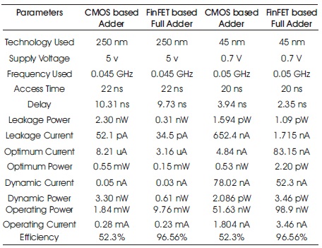
Table 2. Comparative Simulation Results Summary
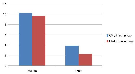
Figure 9. Graphical Representation of Propagation Delay of both type of Full Adders
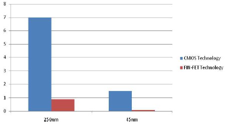
Figure 10. Graphical Representation of Power- Delay-Product of both type of Full Adders
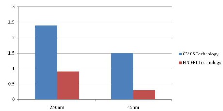
Figure 11. Graphical Representation of Average Power Dissipation of both type of Full Adders
Above two types of 1-bit full adder cells of MOSFET and FinFET were tested and simulated in Tanner EDA to analyse its metric performances, such as propagation delay, average power dissipation, and Power-Delay-Product (PDP). Based on the findings, the 1-bit FinFET-based full adder was shown to be the lowest and optimal trade-off in all metric performances compared to the MOSFET-based full adder. This proved that by using FinFET technology in 1- bit full adder circuitry, it will improve the performance of the device. However, the cell design also contributes to how good the 1-bit full adder performs, as discussed earlier. The 1- bit FinFET-based full adder has a reduced propagation delay and average power dissipation, PDP, thus giving FinFET technology great advantages in energy efficiency and performances for 45 nm technology. It was also verified that the 1-bit Complementary Pass-transistor Logic (CPL) FinFET based full adder performed very well with a reduced amount of PDP compared to other cell designs because of its high-speed performance and full swing operation.
The proposed 1-Bit full adder using FIN-FET technique has some of limition that can be carried out during future work.
These limitations are:
The authors have experimentally investigated the device performance and parameters, such as operating current, operating power, leakage current, leakage power, optimum current, and optimum power transistor count. The previous techniques have a disadvantage of the transistor count and the power dissipation. The current work progresses the design of a 10T full adder using FinFET in which extremely low power dissipation is observed and also the transistor count is low. In this paper, 1-Bit Full Adder using FinFETs has been proposed. The simulations were carried out using Tanner EDA at 250 nm technology.
The simulation results are shown in Table 2 and can be seen that the proposed adder offers improved result. Thus the different types of full adders have been studied and comparison of different full adders in terms of power and number of transistors in various technologies were done. Based on this comparison, 10T full adder is the best power consuming adder. The transistor count is also very low compared to others. This adder is suitable for VLSI applications with very low power consumption. Due to the reduction in a number of transistors, switching activity is reduced. They have also calculated Duty cycle as 96.56%, which is about two times greater than CMOS 1-Bit full adder cell.