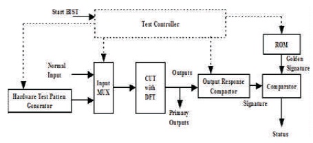
Figure 1. Basic Architecture of ATE
VLSI is the advanced technology mainly intended to incorporate million of transistors or ICs placed on a printed circuit board. As the technology advances, System on Chip (SoC) parameters are scaled to achieve high throughputs. Also different test patterns, Automatic Test Equipment, Automatic test pattern generators are important for testing memory, and device under Test ICs are required to find the faulty chips and hence nesecessary of Automatic Test pattern genetators, which help not only to increase the performance of the circuit, but also increase the life time of the component. In this paper, a high accuracy and wide data rate range pulse generator with 10 ps time resolution is presented to perform Automatic Test. The pulse generator works with two modules like Edge Combiner (EC) and Multi phase clock Generator (MPCG). Edge Combiner focuses on explaining the functionality of data range and timing resolution based on phase selection logic and also down counter. In Multi Phase Clock Generator, a Multiphase Oscillator (MPO) holds a ring oscillator scheme to extend operational frequency. Another advantage of multi phase oscillator is to reduce output phase errors if there is any layout mismatches. The design was implemented on 32 Nanometer CMOS technology with Virtex FPGA is the target Hardware device. Experimental results prove that the Area occupied and power consumed by the proposed pulse generators are found to have Low area and low power consumption, respectively.
Now-a-days, the role of VLSI had became an Essential background for many digital designs range from SmartPhones, Smart TVs to High-end Spatial Applications. VLSI is an important domain which focus on Area occupied by the circuit, Delay incorporated within the circuit and power consumption, where a tradeoff must be made between the ICs to achieve these constraints. VLSI technology allows the designer or a manufacturer to incorporate more transistors of ICs or ASICs or Processors on the single printed circuit board. But the designer side difficulty is to test each component placed on the Printed Circuit Board (PCB). Hence there is a need to develop Automatic Test Pattern Equipments (ATE).
This ATE allows to test the component by itself and authenticate that all the components are free from malfunctioning. The architecture of Automatic Test Pattern Equipment is shown Figure 1.
Figure 1. Basic Architecture of ATE
Hardware Test Pattern Generator: This module generates the test patterns required to identify the faults and propagate the results.
Input Mux: This multiplexer is used to give normal inputs to the circuit when it is operational and test inputs from the pattern generator when BIST is executed. The control input of the multiplexer is fed by a central test controller.
Output response compactor: Output response compacter performs lossy compression of the outputs of the CUT.
ROM: Stores golden signature that needs to be compared with the compacted CUT response. Comparator: Hardware to compare compacted CUT response and golden signature (from ROM).
Test Controller: Circuit to control the BIST. Whenever an IC is powered up (signal start BIST is made active), the test controller starts the BIST procedure.
Earlier, these patterns are not capable of doing test with high precision which results in decreasing the performance of the circuit and sometimes the components disturb the other circuits leading to damage of the entire PCB. In this paper, a Pulse Generator is used that can create test patterns for test chips. In the existing methodologies, the test approach is based on Electronic Test that can generate arbitrary waveforms for measurement of Chips (Tektronix, 2012, 2016; Agilent Technologies, 2009; SRS (Stanford Research Systems, 2006), which is a time and power consuming process. There are some pulse generators not suitable for multi channel applications. To overcome all these problems, a high time resolution pulse Generators operating with 10ps is proposed.
The proposed pulse Generators are implemented by Field Programmable Gate Arrays (FPGA). In this paper, VIRTEX5 FPGA board is selected as target hardware test equipment. FPGA allows the designer to simulate and synthesize code developed before going for ASIC. Other unique features of FPGA devices are that it allows reprogrammable of the code, identify the bugs easily, and can rectify the errors by simulation. To ease the work, the manufacturers often use high performance SoC based chip tester.
Pulse Generators based on Integrated Circuit are often used for IC testing. However, the existing methodologies are lack in high data rate, time resolution, and low power consumption, but highly preferable for wide data range test equipment applications, since the IC type pulse Generator is easy to design for specific applications.
As mentioned earlier in this note, FPGA allows user to simulate the given code, the test is done by programming the FPGA using Hardware Description Language (HDL). FPGA based Pulse Generators can achieve high data rate multi channels and these ICs require high speed and adapts low power requirement (Analog Devices, 2007).
In (Goto, Barnes, & Owens, 1994), to perform Automatic tests a programmable Digital Delay based on shift registers at 1.2 micron CMOS technology is presented. The design is capable of working at 20 MHz operating frequency and comsumes 200 Mw power dissipation and also shift registers are incorporated to reduce power dissipation. In (Miari et al., 2015), a fully integrated eight channel adjustable pulse generator is proposed to overcome delay and to reject electrical disturbances in the circuit. In (Chen, Chen, Lai, & Chen, 2009), to ensure high performance delay, vernier delay lines are constructed by programmable delay lines. This architecture has the advantage of voltage and temperature stability. The existing methodologies include in testing the chips by Timing Vernier Scheme (Kohno, Akiyama, Kato, & Imamura, 2010; Arkin, 2004) aimed to reduce Area and Power for high speed operations. A phase Locked Loop (Wang, Lin, & Tsao, 2004) and Delay Locked Loop [DLL] based PG are also proposed to reduce process, voltage, and temperature variations. In (Okayasu et al., 2006), an active noise controller was also proposed to reduce noise. In (Yamamoto, Suda, & Okayasu, 2007; Ryu, Jung, & Jung, 2013) Pulse Generator (PG) adopts Time-to-Digital convertors to extend time resolution for high end applications. In (Liu & Lee, 2016), fine stage schemes are proposed to achieve low power PG. In this paper, high accuracy waveform, time resolution of 10ps is proposed with operating frequencies range from a few Kilohertz to hundreds of Megahertz.
Pulse Generator is an Electronic circuit or a piece of Electronic Test Equipment as shown in Figure 2, which is used to Generate Rectangular Pulses. PG are mainly used for working with Digital Circuits and Function Generators are used primarly for Analog Circuits. Normally, pulse Generator is preferred to control Pulse Repitition Rate, Frequency, pulse width, delay with respect to efficiency, and the high end low voltage levels of the pulses. More sophisticated pulse generators are allowed to control rise time and fall time of the pulses. Pulse Generators are required for producing response pulses consists of widths, duration, and ranging from one to one pico seconds.
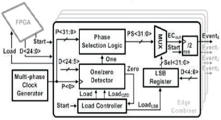
Figure 2. Block Diagram of Pulse Generator
Pulse generators used Analog Techniques, Digital Techniques, or combination of Analog and Digital Techniques to produce pulses. One such example is pulse recycle rate and time may be digitally monitored by the pulse Amplitude and Rise time, Fall time may be described by the Analog circuitry in the output stage of the pulse generator with correct adjustments. Pulse Generators can also produce 50% duty cycle square wave. PG are generally single channel provides one frequency delay with an output.
Pulse generators provide pulses to use in a variety of electronic applications. Some of the functions and capabilities of pulse generator are listed below:
Pulse generators may use either digital or analogue techniques, or a mixture of both. Elements such as triggering and the pulse generation will almost certainly utilise digital technology, but aspects such as the rise and fall time control on the pulse generator are likely to use analogue techniques.
The block diagram of pulse generator (Figure 1) basically comprises of two building blocks, i.e 1. Edge combiner (EC), 2. Multi Phase Clock Generator (MPCG).
The EC consists of the one/zero detector, load controller, multiplexer, divider, and phase selection logic to achieve a small pulse delay time and a small time resolution error (TRE). Its main function is to adjust the phase selectivity in the networks to protect long and heavily load lines. The load controller produces reset signals for each block and also controls the operation of the PG system. The load controller can reset itself by using a delay cell.
It consists of a Phase Frequency Detector (PFD), a Charge Pump (CP), a Low-Pass Filter (LPF), a bias circuit, a Voltage- Controlled Oscillator (VCO), and a divider. The PFD produces an error signal, which is proportional to the phase and frequency differences between F and F . ref back The block diagram fo multiphase clock generator is shown in Figure 3.
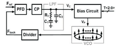
Figure 3. MPCG
Synthesis is the process of converting VHDL or Verilog code into a Gatelevel netlist for the design. If the design contains more than one module, a CPU module is taken as one basic block and RAM is considered as submodule and so on, then the synthesis process generates netlist for each design element. Synthesis process will also check code syntax and summarise the topology of the design. With this one can acknowledge that the design is optimized for the design architecture. The obtained netlist is saved to an Native Generic Circuit file. Xilinx Synthesis Technology is used as a synthesis tool to generate netlist. The logic synthesizer for delay measurement is shown in Figure 4.

Figure 4. Schematic View of Delay Measurement
It is the process of functional verification through timing waveforms. Figure 5 shows the simulation waveforms of the Automatic test pattern Equipment. This is the simulation of On chip Front End Module that contains Signal of Clkin, SamClkin, MuxSel, Vin, Vref signal that produces Output Simulation Waveforms QA, QB. The Delay below Clkin, with 12 Voltage to Delay cell of Vin and 12 Voltage to Delay Cell of Vref Voltage can be Observed by ClkOutA, ClkOutB internal Signal. Based Mux Selection the input, which feed from Register is generated as respective output.
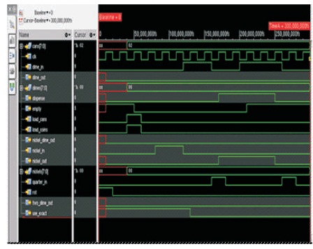
Figure 5. Simulation Waveforms with Faults
A defect is a mistake caused in a device during its fabrication process. The logic values obtained at the device's primary outputs, whereas applying a take a look at pattern to some device under test (DUT). A fault is said to be identified by a take a look at patterns at the output that is the simulation waveforms are totally different than the expected output. In Figure 5, the fault models are observed in the simulation waveforms. The red coloured unwanted waveforms are obtained indicating a fault occurred in the circuit. Figure 6 shows the simulation waveforms of pulse generator indicating ATPG works continuously to identify faults and remove faults during the propogation.
The comparison of results in Table 1 shows that the pulse generator works efficiently than that of the previous methodology.
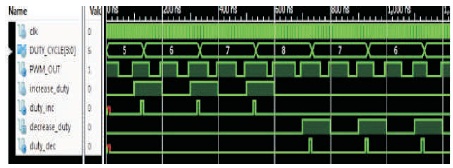
Figure 6. Pulse Generator waveforms without Faults
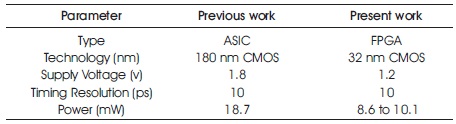
Table 1. Comparison of Results
Due to technology scaling, there is a need to fully integrate ICs on the printed circuit board and ensure the components are working properly without any power losses and thereby need to reduce the complexity of the circuit design engineer and fabrication engineer. In this paper, MPCG-based PG has been proposed for ATE. The PG uses a countdown counter to increase the data rate range. The proposed technique can also reduce the latency of the PG. The MPCG uses a subfeedback loop to obtain high speed with multiphase outputs for a time resolution of 10 ps. For good accuracy of the pulse delay time, the MPCG uses a PEC to reduce the phase errors of the VCO multiphase outputs. The proposed PG was fabricated using a 32-nm CMOS process. The comparison of results shown in Table 1 shows that the proposed design integrated with three circuit techniques achieve a wide operational range and high-accuracy pulse generator. In future, this Built-in Self Test and Automatic Test Equipments enhance the quality of the semiconductor processors and make the technology use for high-end applications.