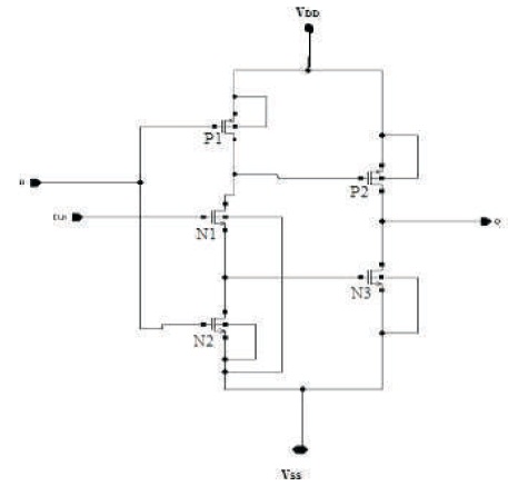
Figure 1. 5T TSPC D-latch
Adders have always been area of continual research in VLSI for high speed data path design. There have been different architectures proposed with design metrics and both the structures are compared for the parameters of power consumption and delay. In the proposed architecture using True single phase clocked (TSPC), D-Latch for square root (SQRT) carry select look ahead adder is compared with Multi-Threshold complementary metal oxide semiconductor (CMOS) D-latch based design. The design shows power dissipation reduction about 56% than that of MTCMOS. Further the proposed architecture using Multi-Threshold TSPCD-Latch for SQRT carry select look ahead adder is compared with Multi-Threshold CMOSD-latch based designs, the design with TSPC shows the power delay product reduction about 11%. Further, the proposed design is compared with different existing carry select adder designs. Hence, the proposed structure which has small area and less power consumption is implemented for 8-bit adder to reduce the power consumption and delay.
In digital circuit design, high speed data path is a topic of constant research with main focus on power dissipation and delay in carry propagation of adder circuit. Some of the adder structures, such as RCA, Carry Look Ahead Adder (CLA), and Carry Skip Adder have either large delay or high-power dissipation leading to inefficient architectures. A compromised structure called Carry Select Look Ahead Adder structure is considered for implementation. In this linear Carry Select Adder, mismatch of speed between inputs and propagated signals creates delay problem, which reduces to some considerable times original by using the Square Root Carry Select Adder. In this structure, a greater number of successive stages are added to eliminate data arrival discrepancy.
Carry select look ahead adder is one of the prominent adders used in data path design today. In (Chang & Hsiao, 1998), researchers have designed a carry select adder using carry ripple adder require 29.2% transistors with speed penalty of 5.9% for bit length of 64 bit. The proposed model achieves 6.3% area saving with same speed. Leblebici (1996) has analyzed and designed the CMOS digital integrated circuits. He, Chang, and Gu (2005) have proposed the design for 64 bit square root carry select adder improves the performance with 44% fewer transistors than the conventional one. Kim and Kim (2001) have implemented low power carry select adder using single ripple carry adder. The proposed structure improves the performance with lesser transistor than the dual ripple carry adder. Ramkumar and Kittur (2011) have designed the carry select adder with low power and area efficient. The proposed structure with CSLA is better than the regular square root carry select ahead adder. Pandey, Bakshi, and Sharma (2013) have simulated and synthesized carry select adder for 128 bit with low power and area efficient. The result reveals that the proposed structure reduces area and leakage power with no delay. Mugilvannan and Ramasamy (2013) have proposed the design of carry select adder using modified BEC-1. The result reveals that CSLA structure shows better performance than the ordinary SQRT CSLA. Shanigarapu and Shrivastava (2013) have designed the carry select adder with area and power efficiency. The proposed design is reduced with area and power compared to modified CSL adders. Priya and Kumar (2013) have implemented and compared the efficient architecture and area for CSLA. The proposed architecture reduces the area for CSLA. Akashe, Tiwari, Shrivas, and Sharma (2012) have proposed a novel high speed low power half adder cell. The result reveals that half adder reduces leakage power compared to CMOS technique. Manju and Sornagopal (2013) have observed that by replacing BEC-1 based design with Common Boolean Logic (CBL) will reduce the delay, but still there is appreciable PDP. From (Naik, 2015), selecting carry before final sum calculation will reduce power dissipation, but delay is increased. From (Das, Mandal, & Das, 2015), it is observed that replacing BEC-1 with D-Latch, the Power Delay Product (PDP) will decrease. But, there is still large power dissipation due to large transistor count. The authors propose that by replacing NAND based D- Latch with TSPCD- Latch will further improve the power delay product, as transistor count decreases in the proposed architecture (Asthana & Akashe, 2013). In order to reduce dynamic power dissipation, multi-threshold technique (MTCMOS) was proposed in (Asthana & Akashe, 2013) and result shows appreciative decrease in PDP with MTCMOS based design. Hence, by applying multi-threshold for TSPCD-Latch, delay associated with design is decreased in order to achieve lesser PDP.
The authors have implemented the 8-bit SQRT CSLA using TSPCD - Latch and MTTSPCD - Latch. These implementations are discussed in the following sections.
This implementation uses TSPC D-Latch by replacing the NAND based D-Latch (Asthana & Akashe, 2013).
2.1.1 TSPCD-Latch
TSPC stands for True Single-Phase Clocked logic in which we only have one clock, and do not need an inverted clock. TSPC circuit technique uses single phase clock and hence, to avoid the skew problems, and thereby improves the performance of a digital system. There are several benefits with this technique, which are
Figure 1 shows the schematic of 5T TSPC D Flip Flop, which is composed of 3 NMOS and 2 PMOS transistors. When CLK and input 'D' are high, transistors P1, N3 are OFF and remaining transistors P2, N1, N2 are ON and the output becomes high. During ON clock period, whatever is the value of input it reaches output. During OFF clock period, previous output is retained. The output waveform is shown in Figure 2.
Figure 1. 5T TSPC D-latch
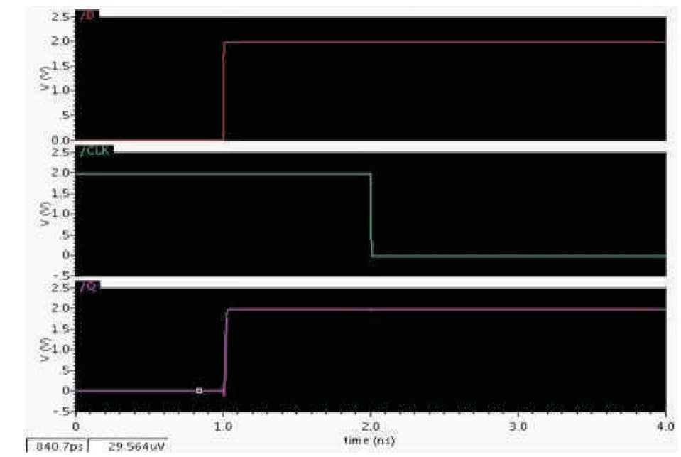
Figure 2. Output Waveform for TSPC D-Latch
2.1.2 Proposed Structure for 8-bit SQRT CSLA using TSPCD-Latch
The proposed structure for 8-bit implementation consists of the following blocks as shown in Figure 3.
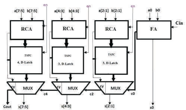
Figure 3. 8-bit Implementation
Cadence implementation of the proposed 8-bit structure is designed and simulated using 90nm technology. Pro_tspc1 is proposed 2 and 3-bit implementation with 'control carry' as the control signal for carry to generate sum for either carry '1' or '0'. Figures 4 and 5 show the proposed 2- bit implementation and 3-bit implementation, respectively. 'd_ll' is a proposed TSPCD- Latch.
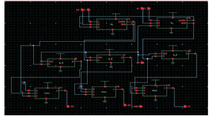
Figure 4. 2-bit SQRT CSLA using TSPCD-Latch
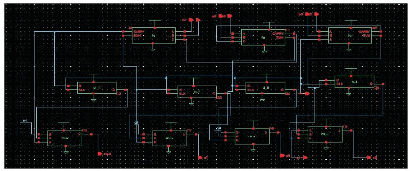
Figure 5. 3-bit SQRT CSLA using TSPCD-Latch
Figure 6 shows 8-bit implementation of the proposed structure using TSPC D-Latch. Figure 7 is the output for carry '0' and '1’.
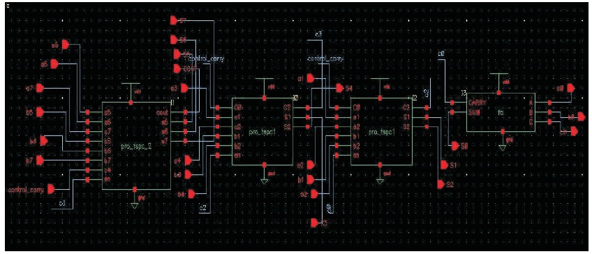
Figure 6. 8-bit SQRT CSLA Based on TSPC D-Latch
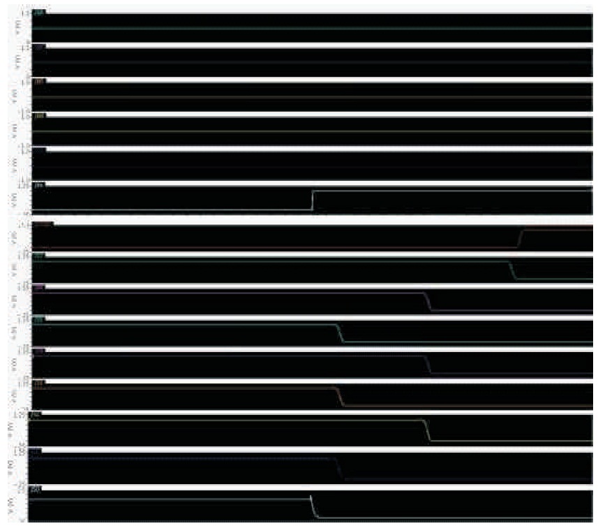
Figure 7. Output for 8-bit TSPC D-Latch based SQRT CSLA
2.1.3 Experimental Observation
The proposed design using TSPC D-Latch results in less power dissipation compared to (Asthana & Akashe, 2013), but delay in carry propagation is slightly increased as shown in Table 1. To overcome the delay problem following design is proposed.
This implementation uses Multi-Threshold TSPC D-Latch in place of MTCMOS D-Latch.
2.2.1 MTTSPCD-Latch
Multi-Threshold TSPCD-Latch represents modified Multi- Threshold CMOS (Leblebici, 1996) D-Latch. As in the case of MTCMOS D-latch, MTTSPC D-latch has two sleep transistors controlled by 'SL' and 'SLB', respectively. Figure 8 shows simulated MTTSPCD-Latch and the corresponding output is shown in Figure 9. Figures 10 and 11 represent block level 2-bit and 3-bit implementation of the proposed architecture, respectively.
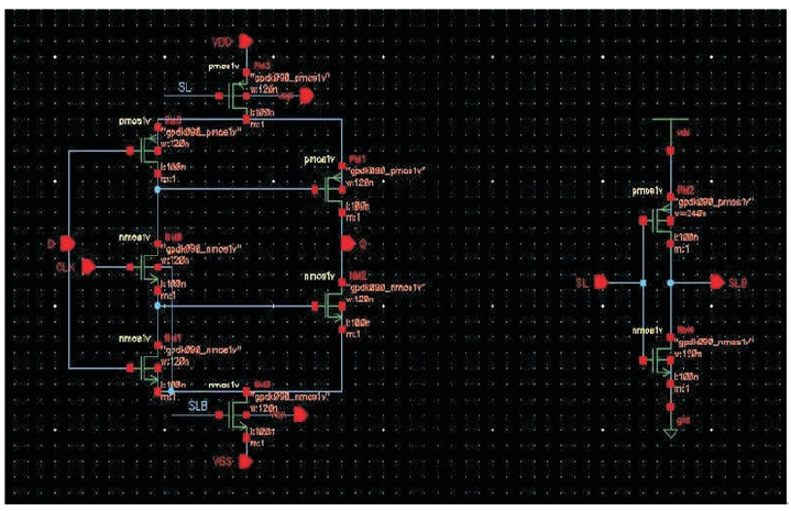
Figure 8. MTTSPC D-Latch
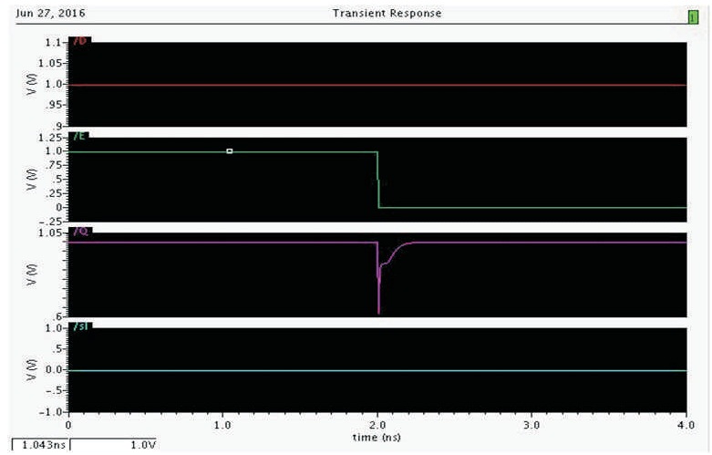
Figure 9. MTTSPC D-Latch Output
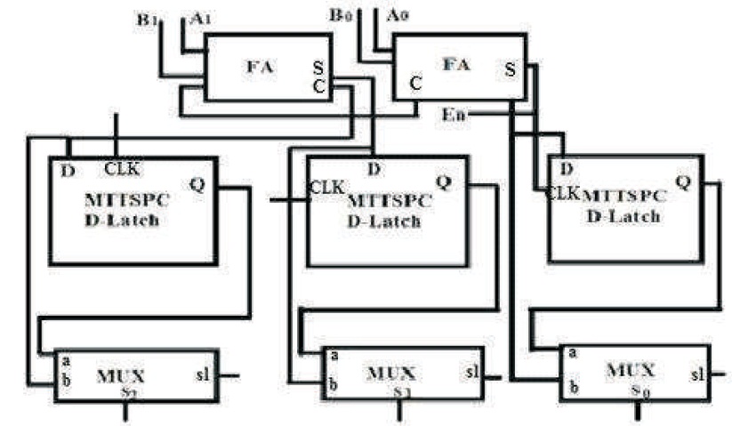
Figure 10. 2-bit Implementation
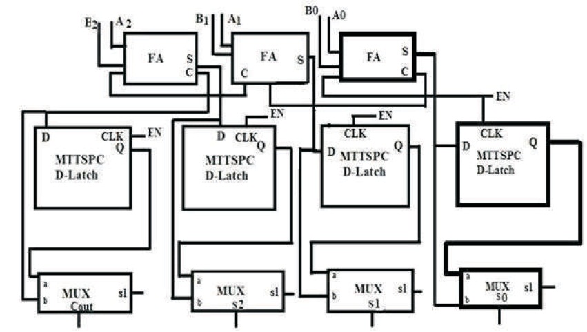
Figure 11. 3-bit Implementation
2.2.2 Proposed Structure for 8-bit SQRT CSLA using MTTSPCD-Latch
The proposed structure for 8-bit implementation consist of the following blocks as shown in Figure 12.
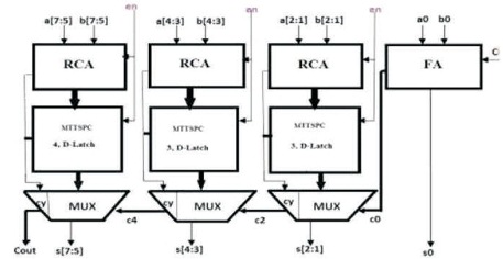
Figure 12. 8 Bit Implementation
Here ‘en’ is pre-assumed carry (either 0 or 1), based on which sum and carry is calculated. c0, c2, c4 are carry select line for multiplexer unit.
Figure 13 is the proposed structure of 2 bit square root CSLA using MTTPSC represents modified multi-threshold Dlatch and implementation details are as explained before. enispre - assumed carry 0/1 based on which sum and carry is calculated. C4 is carry select line for multiplexer unit.
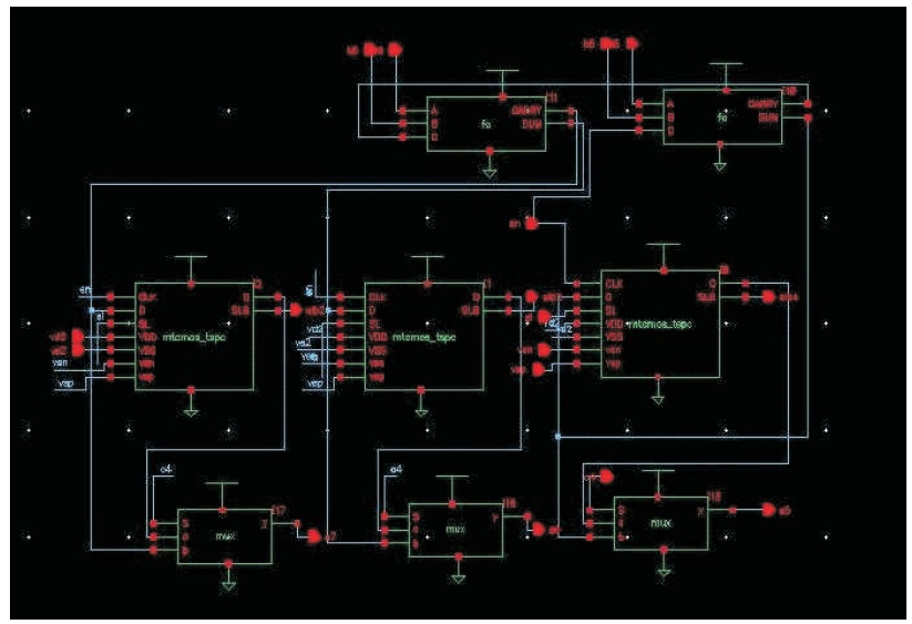
Figure 13. 2-bit SQRT CSLA Using MTTSPC D-Latch
Figure 14 is the 2-bit implementation extended for 3-bit implementation with full adder, additional multiplexer, and MTTSPC D-latch is included for the proposed structure. The proposed structure for 8-bit implanted is shown in Figure 15. Replacing MTCMOS D-latch with multi-threshold TSPC D-latch in order to decrease power-delay product is done in two steps. First is replacing normal D-latch with TSPC D-latch, second is to add sleep transistors to the Dlatch. In cadence implementation, MTCMOS-TSPC is the proposed D-Latch using multi-threshold technique. 'VSN', 'VSP' are threshold control for TSPCD-Latch and 'sl' is control for high VT sleep transistor. Figure 16 is the Cadence simulation output for Vin='1' and carry=0/1. Delay is calculated from carry in to carry out.
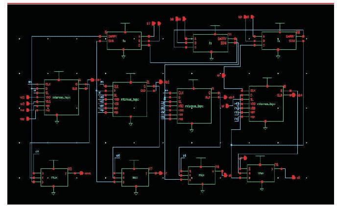
Figure 14. 3-bit SQRT CSLA Using MTTSPC D-Latch
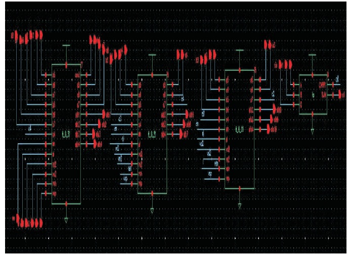
Figure 15. 8-bit SQRT CSLA Using MTTSPC D-Latch
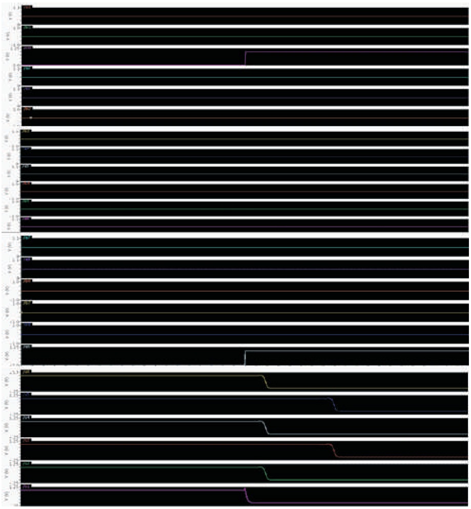
Figure 16. Output for 8-bit MTTSPC D-Latch based SQRT CSLA
In the proposed structure, the gate count is less as compared to the MTCMOS D-Latch based SQRT CSLA. This analysis shows that the proposed structure has less power dissipation, although delay remains the same compared to former. The proposed architecture using,
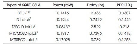
Table 1. Comparison of different architecture in terms of design metrics @ , *Proposed architectures, Kim & Kim, (2001) $ Asthana & Akashe, (2013)
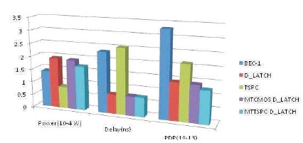
Figure 17. Comparison of Results for Different Implementation
With the elevation of silicon technology, it is becoming convenient for compression system to effectively implement carry select adder using MTTSPC D-latch with an initial proposal with less power and delay. In future, the power and delay parameters without penalty of resources are reduced with different modifications and advancement with new technology nodes.
The performance analysis and the different types of architecture are compared. To reduce the Delay of TSPC D-Latch based SQRT CSLA architecture, MTCMOS D-latch based SQRTCSLA is used and it is compared with modified CSLA (TSPC) and D-latch based CSLA. Next, MTTSPCDLatch based SQRTCSLA is compared with MTCMOSDlatch. All these adders are evaluated for 8-bit SQRT CSLA in terms of Delay, Power, and Power-Delay Product (PDP) in Cadence Virtuoso environment 90nm CMOS process technology in room temperature and the proposed structure has shown better result in terms of delay and PDP. There are several leading advantages with proposed circuit, which eliminates the clock skew and saves area power consumption. Furthermore, it can be implemented in many applications, such as converters, microprocessors, and clocking systems.