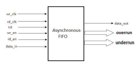
Figure 1. Schematic Symbol of Asynchronous FIFO
A First in First out (FIFO) is used as a memory buffer between two asynchronous systems with simultaneous write and read access to and from the FIFO, where these accesses being independent of one another. Sequential operation of FIFO is particularly useful for implementing system level functions like Packet Buffering, Frequency Coupling, and Bus Matching. Asynchronous FIFO is a memory file, which uses synchronization for reading and writing with different clocks, by performing the conditions of over-run and under-run. In essence, the transfer of data from read domain to write domain with different frequencies. To generate overrun and under-run status flags, the synchronization takes place with the help of “preceding operation”of both the write and read pointers. In this design, the gray code converters are used to reduce switching activity and the low power Design for Testability (DFT) technique was applied by considering the two phases that is scan insertion and ATPG Simulations. This design is executed by using synthesizable VERILOG (Register Transfer Level) RTL Code and verified with Xilinx ISE simulator.
First in First Out is a memory file that allows the data in a queue and it uses the synchronization for transferring the data. In this paper, low power DFT is implemented by using the Asynchronous FIFO. FIFO can be differentiated in two ways (Anumothu, Kishore, & Reddy, 2016):
1. Synchronous FIFO
2. Asynchronous FIFO
In synchronous FIFO, data is steered into and out of the memory array by two pointers, i.e., read pointer and write pointer, respectively. After completion of each operation, the particular pointer is incremented to allow access to the next address pointer in the sequence of an array. By using the single clock, the read and write operations are performed by using same frequency, whereas in asynchronous FIFO, two clocks are needed for read and write pointers, where both the pointers are needed to be accessed with two separate clock frequencies. One clock is used for composing the data in to the memory and another clock for reading the data from the memory.
The concept in this paper is to reduce the power consumption using DFT (Design for Testability) by implementing the novel architecture of asynchronous FIFO by synchronizing the read and write pointers and generating the overrun (FIFO_FULL) and underrun (FIFO_EMPTY) conditions with the help of “preceding operation”.
Figure 1 depicts the schematic figure of an Asynchronous FIFO and its architecture is shown in Figure 2. The input signals are shown below:
Figure 1. Schematic Symbol of Asynchronous FIFO
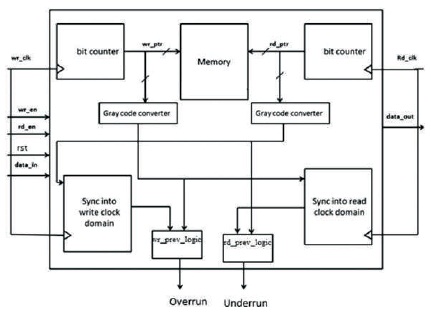
Figure 2. Architecture of an Asynchronous FIFO
The output signals are:
In Asynchronous FIFO, two clocks are used with different frequencies. wr_clk and rd_clk indicate the write clock and read clock respectively, whereas the write and read operations are performed by using those two clock signals. Both the read and write clocks are used for the write and read operations, respectively with different frequencies. Rst indicating the resetting signal is used to reset the FIFO to the known state. Write operation is formed if and only if wr_en is high, which is similarly for the Read operation also. Data_in is input signal used for writing the data into the memory, and Data_out is the output signal used for reading the data from memory. Here the two status flag generations i.e., Overrun and Underrun conditions, which are proposed to prevent the overflow (writing the data inside the FIFO) condition requests the write data after completion of total address lines in the FIFO. Underrun is proposed to prevent the underflow (reading the data from the FIFO) condition that is requesting the read data after the FIFO is empty.
This paper discusses the detailed architecture of Asynchronous FIFO which is different from the other designs. As the entire architecture was designed using only with the help of mux's and flip flops.
Before designing the FIFO, one should study and clearly understand the read and write pointers in a FIFO, the entire operation is dependent on the pointers itself. Here these pointers address memory locations. So, it is better to consider pointers and shift them accordingly instead of shifting the data that is to be written or read from one address location to another. So, there is a reduction in circuitry and complexity. This makes an efficient design.
Firstly, the read and write pointers are placed at the initial positions of the address locations and then these pointers are incremented according to the assertion of read enable and write enable signals. In this paper, the memory specified was “n” number of address locations and of m-bit wide data. After completion of read operation, the read pointer will immediately point to its next address location, similarly for write operation too. After addressing all the “n” number of address locations, the pointer comes to its initial state depending upon the enable signals. If the data is continuously written into the memory and the performance of read operation has not occurred, then the write pointer will come to its initial state and will remain in the same state, even though the write enable signal is asserted. Similarly, it is for read pointer too.
Here the synchronization of read and write pointers will take only with the help of “Gray Code Converter” and for the other characteristics if the Gray code converter will become an importance in representing the successive binary numbers and it is shown in Table 1. For each binary increment there is reflection only with one bit change, thus reducing the switching action and hence power. This lower switching action accomplishes to less glitch formation and thus reducing any meta-stability (Ramesh, Kumar, & Reddy, 2012).
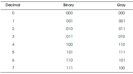
Table 1. Gray Code Sequence Conversion
When comparing the two pointers (representing 5-bit read and write address), reduction of meta-stability will come to an importance, the possibility of interpreting a signal transition from 1 to 0 or 0 to 1 as 0 s and 1s, respectively (Mudavath & Kishore, 2016). The number of transitions will be reduced by the combinational logic (XNOR gate as an equivalency check) which in turn becomes easier (Hussain & Kishore, 2016).
In general, the over-run and under-run conditions are generated based on the read and write position pointers (Kishore, Akhil, Viswanath, & Kumar, 2016). Here the synchronizer circuit performs the mechanism of by reading the gray code write pointer with read clock domain and the gray code read pointer with write clock domain. Hence there is a need of synchronizing circuit and Figure 3 depicts the synchronization mechanism.
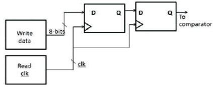
Figure 3. Synchronizer Circuit
Here a one bit data is synchronized using two flip flops. The read data is synchronized with write clock and write data is synchronized with read clock.
From Figures 4 and 5, it is clear that the over-run and under-run conditions, respectively are generated by last operation logic and the comparison of gray code pointers using a comparator with synchronization of read pointer with write clock and the write pointer with read clock pointer. And both the comparisons between read and write gray code pointers are done as follows:
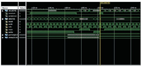
Figure 4. Over-run Status Flag Generation
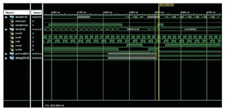
Figure 5. Under-run Status flag generation
The Scan Insertion and ATPG Simulations (Gopal & Kishore, 2016) are introduced out in the existing architecture. The paper divides the scan clock for even and odd scan chains, thereby reducing the power constraints using the Low Power DFT (Dastagiri & Kishore, 2016a, 2016b). The power constraints will be considering into three appropriate conditions as shown in Figure 6. Firstly, the two techniques are applied to different locations in the implemented architecture and thereby considering the double edge triggering method. Then the power will be reduced from previous existing DET method to an extent of 0.00032 W to 0.00027 W, whereas from DET method to considering the frequency by halving the total hierarchy power will be utterly diminished to a greater extent of 0.00009. Table 2 shows the device utilization summary.
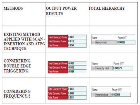
Figure 6. Power Comparison by Considering Three Techniques for Proposed Architecture
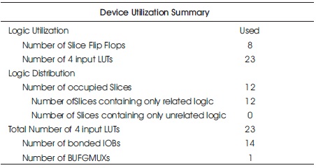
Table 2. Device Utilization Summary
Asynchronous FIFO considering over-run and under-run conditions were implemented using xilinx ISE. This implementation was novel since over-run and under-run conditions helped in generating status flags with the help of a signal i.e., previous operation. The Gray Code Counter employs in using a comparator along with the preceding operation for the generation of over-run and under-run status flags. Continuous writing of data into the memory, continuous reading of data from memory, and simultaneous reading and writing from the memory are verified with different test cases. All these test cases are verified using Xilinx ISE Simulator. The work involves employing scan insertion and ATPG flow. The power analysis of the double edge triggered FIFO was done with reference to available Asynchronous FIFO with Scan insertion and ATPG. It was observed that there was 15.62% power reduction. It was also compared by halving the frequency with reference to double edge triggered. It was observed that there was 66.6% power reduction. Finally, the power was reduced by 71.87%.
The work can be extended in future by implementing the design by using the existing techniques like BIST (Built in Self Test) (Charan & Kishore, 2016) for the self-testing analysis and for the reduction power consumption, the CPF (Common Power Format) and the UPF (Unified Power Format) will be preferably using SYNOPSIS tool for better results.