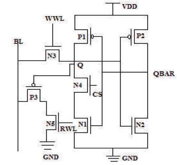
Figure 1. Proposed 8T SRAM circuit
Design and implementation of memory devices are becoming a challenge for the memory designers due to various limitations. Leakage power dissipation and low data stability are the main constraints, while designing memory integrated circuits. In this paper, a new 8T Static Random Access Memory (SRAM) cell, that adopts a single bit line scheme has been proposed to limit the leakage current as well as to gain high data stability. The proposed circuit consumes 671.22 pA leakage current during idle state of the circuit. It shows the high data stability 343 MV and 329 MV during read and hold state, respectively. Additionally, this paper contains 64-bit memory unit of the proposed 8T SRAM cell (8 x 8) array. The array comprises of row decoder, column decoder, and sense amplifier. The proposed 8T SRAM cell is 16.45X and 43.78X fast during read 0 and read 1 operations, respectively, while during write 0 and write 1 operations the delay is reduced up to 8.05% and 8.46%, respectively when compared with (8 x 8) array of 6T SRAM cell. During read 0 and read 1, it is fast by 16.45X and 43.78X, respectively. The average power consumption during read 1/0 and write 1/0 operations are 99.5% /60.05% and 99.61% /59.82% less as compare to 6T SRAM array, respectively.
Modern integrated circuits demand continuous down scaling of process technology, which leads to higher integral density and challenges to improve the performance of the device (Grossar et al., 2006). In recent technology, SRAM has dominated part of the chip design. That is facing severe problems like power dissipation, leakage current, and stability (Seevinck et al., 1987; Wen et al., 2013). Supply voltage minimization can reduce total power dissipation, but it affects adversely on the stability of the cell. Hence degrades the static noise margin of the cell (Roy & Prasad, 2000). Due to this limitation, it becomes difficult to operate the conventional 6T SRAM cell at low power supply. The conventional 6T SRAM cell has a limitation of reading disturbance during read operation (Chang et al., 2008), which results in poor read static noise margin. The read static noise margin can be improved by totally disconnecting the bit lines from the storing nodes. This can be achieved by using differential word-lines for write and read operations (Kushwah et al., 2014). Due to single bit-line, the average power dissipation and leakage current can be minimized to some extent (Wen et al., 2013; Tu et al., 2010).
In this paper, the 64-bit memory unit (8 x 8 array) of the proposed 8T SRAM cell has been designed. The array consists of many peripheral circuits, such as decoders, write assist circuits, and sense amplifier to read the stored data bit (Roy & Prasad, 2000; Wen et al., 2013). The decoder is used for decoding the physical address of the cell provided by the processor. The sense amplifier is used to read and amplify the stored information of the selected cell (Amrutur & Horowitz, 2001).
In this paper, a single ended 8T SRAM cell is explained for arranging the low leakage current and high data stability in the sleep mode of the circuit design. The utilized cell is shown in Figure 1, which provides the 70 nm technology. The cell is confident of two cross coupled inverters P_1, P_2, N_1, and N_2 and approaches the transistor N_3. The information is stored on the storing nodes Q and QBAR. An additional charge in the storage transistor CS (N_4) is used to disengage the feedback loop in the active mode of the circuit that will used to increase the establishment of the cell as it restricts the data flip mechanism during different modes of operation (Kushwah et al., 2016; Raikwal et al., 2017). Hence this eliminates flipping of content, which occurs suddenly in conventional 6T SRAM cell and enhances the data stability of the cell. The simulation results of the proposed system is shown in Table 1.
Figure 1. Proposed 8T SRAM circuit

Table 1. Simulation Results of Proposed 8T SRAM Cell
In idle mode of the cell, Write Word Line (WWL), Read Word Line (RWL), and charge storage transistor CS are maintained at ground level. The hold operation CS is kept turned off to compress the leakage current. In the sleep mode of the cell, robust data stability is repeated as well as with low leakage current.
Prior to write operation, BL is charged to VDD or discharged to 0 V depending on what is to be written '0' or '1' on the storing node Q. Before initiating single ended write operation WWL is charged to VDD and RWL is maintained at 0 V. Charge storage transistor CS is kept at 0 V, to enhance the write stability of the cell during write state. The OFF state of CS helps to restrict the charge flow from node Q to ground. Data is written from bit line to the node 'Q' through WWL. Due to separate word lines, data stability is improved (Zhang et al., 2005). The chance of data distortion is eliminated by keeping CS turned off.
Before initiating single ended read operation, BL is charged to VDD . Signals RWL and CS are given as a transition to VDD while WWL is discharged to 0 V. In this cell, the storing node Q is directly connected to the PMOS (P_3) transistor. Assume that '1' is stored on node Q, BL will not get discharged because the P_3 transistor is in the cut off state (Zhang et al., 2005). Therefore, the charge stored at BL is directly accessible by the sense amplifier and recognize as '1', otherwise, when '0' is saved at node Q, the P_3 will turn ON. RWL is in active state, BL is discharged through P_3 and N_5 and '0' is sensed by the sense amplifier.
In this section, 8 x 8 SRAM array has been designed with the help of peripheral circuitry. The array consists of row decoder, column decoder, and sense amplifier. The row and column decoder are implemented using NAND gates. Due to single ended SRAM cell, the single ended sense amplifier is used.
To design 64-bit memory unit, 3:8 decoder is essential. The row decoder internally decodes the given input address given by the processor and selects the word-line to be accessed (Amrutur & Horowitz, 2001). The number of word lines are equal to the number of rows in SRAM array. In this array, there are 8 rows and with each row, 8 cells are associated. The row decoder selects one of the row depending on the input combination. A bit of data can be read or written by selecting the address. The decoder consists of NAND gates, which is relatively faster. The signals A, B, C are the inputs and A0 to A7 are the outputs of the row decoder. Figure 2 shows the diagram of row decoder, column decoder, and sense amplifier.
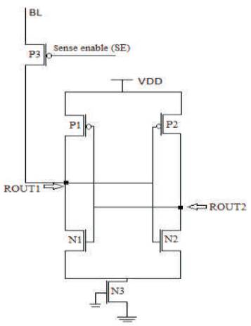
Figure 2. Schematic of Single Ended Sense Amplifier
In order to implement 8 x 8 memory array, 3:8 column decoder is required. Column decoder activates the bit line by proper combination of the input bit pattern. As row decoder, column decoder internally decodes the given input address and selects the bit-line to be accessed. There are 8 columns and with each column, 8 cells are associated. The signals X, Y, Z are the inputs and X0 to X7 are the outputs of the column decoder. A bit of data can be read or written by giving the proper address through row and column decoder.
Sense amplifier is a vital component in the memory design. The design and the internal construction of sense amplifier depicts the read speed and the power dissipation of the cell during read operation. Sense amplifier produces the voltage difference of both the Bit- Lines BL and BLBAR and amplifies it while performing the read operation. While reading the content of memory cell, one of the Bit-Line gets discharged. The sense amplifier senses the voltage difference between both the bit-lines and amplifies it to the desired voltage level. Afterwards, the amplified signal is recognized as 0 or 1. The sense amplifier senses the very low voltage difference of approximately 50 mV and the ability to amplify the signal to be recognized as logic '0' or '1' (Yang & Kim, 2005).
Furthermore for sensing the stored content of single ended 8T SRAM cell, single ended sense amplifier is utilized. Bit Line (BL) of the memory cell acts as an input to the sense amplifier. Sense-Enable (SE) input is used to activate the sense amplifier to access the stored bit. Initiation of read operation is started while BL is precharged to supply voltage (VDD) and the SE signal is activated to enable sense amplifier. If logic '1' is stored at the storing node, the stored charged get discharged through the BL. The single ended sense amplifier senses the voltage difference between the storing nodes Q and QBAR. Hence the stored bit of the memory cell is available at the output nodes ROUT1 and ROUT2 of the sense amplifier. Figure 2 depicts single ended sense amplifier utilized in 64-bit memory of 8T SRAM cell to read the stored bit.
The size of memory unit is designed according to the need of applications. The design should fulfil the performance requirement in terms of different parameters, such as speed, power dissipation, and stability. To design the memory unit, various peripheral circuits are required to design. The 64-bit array is implemented using 64 numbers of proposed 8T SRAM cell. The array consists of 8 rows and 8 columns, therefore it is capable of storing 64-bits of data (Grossar et al., 2006). Figure 3 represents the block diagram of 8 x 8 memory unit, whereas Figure 4 shows the schematic of 64-bit memory unit.
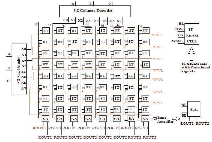
Figure 3. Block Diagram of 64-bit 8T SRAM Cell
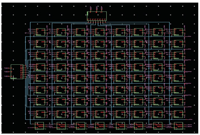
Figure 4. 64-bit 8T SRAM Cell Memory Unit
Row decoder activates the word-lines by decoding the input bit (A, B, C) combination, whereas column decoder enables the Bit-Line of the selected cell depending on the input bit (X, Y, Z) combination given by the processor. Depending on the addresses of the row and column decoder, a cell is selected to be read or written. Address given by the column decoder allows to select the sense amplifier. Stored data of the selected cell becomes available to be sensed by the sense amplifier (Hua et al., 2005). The sense amplifier senses the voltage level and produces the outputs as ROUT1 and ROUT2. The single ended sense amplifier is used with 64-bit memory unit of the proposed 8T SRAM cell.
In this section, the utilized technique 8T SRAM cell is implemented and assessed. The circuit is distinguished by using the 70 nm technology with the supply voltage of 1.2 Volt. Circuit validation is done on the Tanner tool. Representation of the SRAM cell is designed on the S-Edit and net list result is done by using T-spice.
In this section, average access delay of 8T SRAM (64-bit memory unit) is compared with an average access delay of conventional 6T SRAM (64-bit memory unit). Tables 2 and 3 give the delay values where Figure 6 illustrates the graph of access delay at different address combination of row decoder. Read-write waveform of the proposed 8T SRAM cell (8 x 8) array is shown in Figure 5.
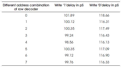
Table 2. Access Write '1' and Write '0' Delay for Different Address Combination of 64-bit Memory Unit
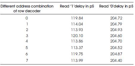
Table 3. Access read '1' and read '0' Delay for Different Address Combination of 64-bit Memory Unit
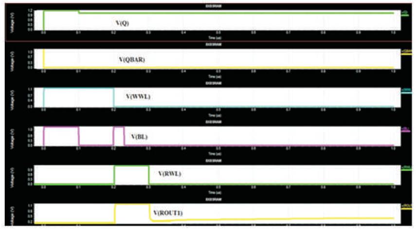
Figure 5. Read-Write Waveform of Proposed 8T SRAM Cell (8 x 8) Array
The write and read delay analysis of the SRAM memory unit for the desired word is calculated by selecting proper addresses through the row decoder and column decoder. It is evaluated by the 50% rise of writing a wordline voltage to the 50% fall of available voltage at Q and QBAR.
Similarly, the read delay of the memory unit is evaluated for the selected bit by the addresses applied by the row decoder and column decoder. The selected cell content is read by the sense amplifier. The read delay of the cell is also dependent on the addresses given by the decoders. It is calculated by a 50% rise of read word-line to the 50% fall of sense amplifier output. Table 4 shows the comparison of access read/write delay for 64-bit memory unit of 6T SRAM cell and 8T SRAM cell. Figure 6 depicts the read and write access delay graph for 64-bit memory unit of 6T SRAM cell and 8T SRAM cell.
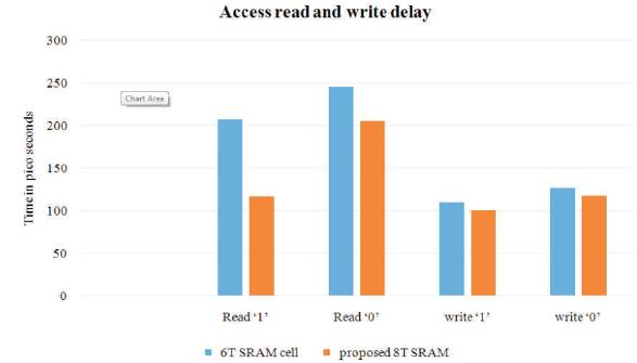
Figure 6. Comparison of Read and Write Access Delay
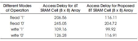
Table 4. Comparison of Access Delay for 64-bit Memory Unit
In this section, average power dissipation of both (8 x 8) array is calculated and compared. Table 5 gives the values of average power dissipation during different modes of operation, whereas Figure 7 depicts the comparison graph.
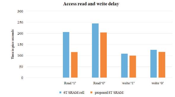
Figure 7. Comparison of Average Power Dissipation
Table 5 and Figure 7 depict the values and graph of average power dissipation for memory unit during different modes of operation, i.e. read '1', read '0', write '1', and write '0'. It is concluded that 8T SRAM cell memory unit consumes less power in every mode of operation as compared to the memory unit of the conventional 6T SRAM cell. The low power dissipation is achieved for proposed 8T SRAM cell memory unit utilizing a single bitline and single ended sense amplifier.
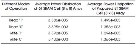
Table 5. Comparison of Average Power Dissipation for 64-bit Memory Unit
The design of the SRAM memory unit is taken into consideration in this work. The speed and average power dissipation of SRAM cell is calculated. The operation of different peripheral circuits is verified and analyzed in this section. The implementation of different peripheral circuits, including row and column decoders and sense amplifiers is discussed. The proposed circuit consumes 671.22 pA leakage current during idle state of the circuit. It shows the better data stability of 343 MV and 329 MV during read and hold state, respectively. Additionally, this paper contains 64-bit memory unit of the proposed 8T SRAM cell (8 x 8) array. The array comprises of row decoder, column decoder, and sense amplifier. The proposed 8T SRAM array is 8.05% and 8.46% faster during a write '0' and write '1', respectively when compared with (8 x 8) array of 6T SRAM cell. While during read '0' and read '1', it is fast by 16.45X and 43.78X, respectively. The average power consumption during read 1/0 and write 1/0 operations are 99.5% /60.05% and 99.61% /59.82% less compared to 6T SRAM array, respectively.