Figure 1. MESFET Structure
In this paper, the authors present a comparison through a simulation study, among different hetero structure devices, like Metal Semiconductor Field Effect Transistor (MESFET), High Electron Mobility Transistor (HEMT), and Tunnel Field Effect Transistor (TFET), with reference to their applications in electronic field. In particular, MESFET and HEMT present good performance in power amplifiers and they are characterized by high mobility of the charge carriers that allows to consume less at high frequency. TFET is the newest experimental device, which has a very powerful application in logic circuits, ultra low-power specific analog ICs with better temperature strength and low-power SRAM.
Homo-junction devices have some consistent limitation that reduces their field of applications (Perri, 2016; Marani & Perri, 2015) because, during the fabrication process, characteristics like potential barriers, spatial distribution, and carrier transport cannot be controlled independently.
Electronic devices based on heterostructure combine different semiconductor materials, obtaining more useful and interesting characteristic. For example, GaSb in contact with InAs present non-overlapping band gaps, while, in AlSb-InAs and GaSb-InAs system, the conduction band is particularly large and this is useful to make deep quantum wells and high tunnelling barriers.
In this paper, the authors present a comparison through a simulation study, among different heterostructure devices, like MESFET, HEMT, and TFET, with reference to their applications in electronic field. In particular, the simulated devices are compared to typical MOS device in order to evaluate the differences in power, telecommunication, and digital electronic applications.
After a brief description of the operation principle of the examined devices, the authors propose numerous simulations of electronic circuits using these devices, discussing the obtained results.
In particular, the MESFET and HEMT present good performance in power amplifiers and due to high carrier mobility, it consumes less at high frequency. Regards to TFET device, the authors show that, it has a very powerful application in logic circuits.
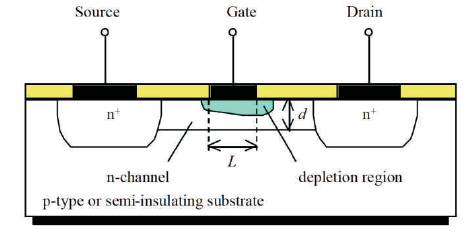
Figure 1 shows the MESFET structure (Marani & Perri, 2015), where the base material on which the transistor is fabricated in a semi-insulating GaAs substrate. A buffer layer is epitaxially grown over the semi-insulating substrate to isolate defects in the substrate. The channel or the conducting layer is a thin, lightly doped (n) conducting layer of semiconducting material epitaxially grown over the buffer layer. Finally, a highly doped (n+) layer is grown on the surface to aid in the fabrication of low-resistance ohmic contacts to the transistor.
The key advantage of the MESFET is the higher mobility of the carriers in the channel as compared to the MOSFET (Prasertsuk et al., 2016). The effect of the high mobility makes this device useful in microwave applications or other fields whose high work frequency is required. On the other side, the side-effect of this device is the effect of the Schottky metal gate which limits the forward bias voltage on the gate to the turn on voltage of the Schottky diode (Marani & Perri, 2015). The threshold voltage therefore must be lower than this turn-on voltage. As a result, it is more difficult to fabricate circuits containing many enhancement-modes in MESFET.
Figure 1. MESFET Structure
Firstly, a JFET Class B output stages (Figure 2) is simulated as an element of comparison. This configuration presents advantage in terms of power, but it is not a perfect voltage follower. Figures 3 and 4 show In-Out voltages and the output characteristic of the JFET push-pull, respectively.
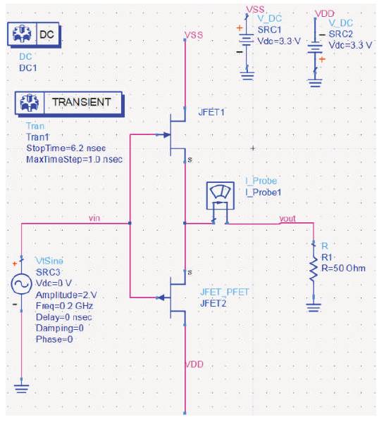
Figure 2. JFET Push-Pull Output Stage
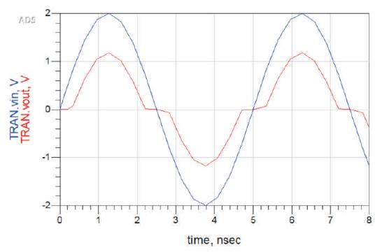
Figure 3. Input and Output Voltages Versus Time
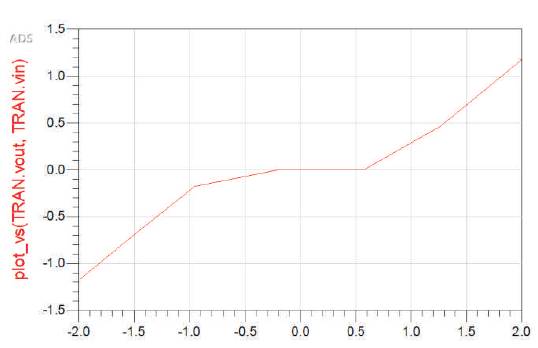
Figure 4. Output Characteristic of JFET Push-Pull Stage
A comparison with the MESFET is possible through the circuit in Figure 5.
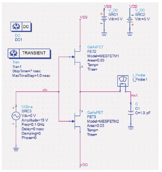
Figure 5. MESFET Push-Pull Output Stage
In Figure 6, the output characteristic is shown, emphasizing that the MESFET model used in these simulations is that of Curtice’s simulation (Curtice, 1980; Statz et al., 1987).
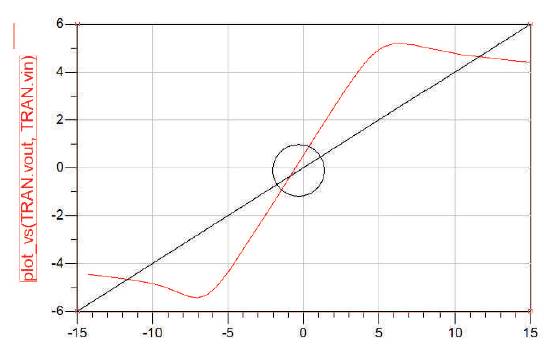
Figure 6. Characteristic of the MESFET Push-Pull
With reference to Figure 6, the black line represents a reference that passes from the origin of the axis and cuts the graph in two equal parts. On the top and the bottom of the graph, the characteristic is limited by the value of the source Vdd and Vss , respectively.
Figure 7 shows the typical offset from zero of the class B output stage.
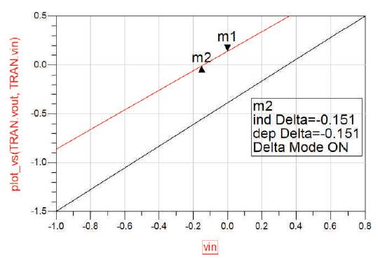
Figure 7. Focus on the Origin
Marker m1 indicate zero, m2 is on the point when the characteristic cross the zero, equal to -0.151 V. A better setting on the circuit design and the characteristic for negative Vgs on the MESFET, produce the result described through Figure 8. Near the zero there is a very little offset that result in insignificance with respect to the JFET case.
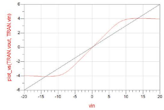
Figure 8. Improved Characteristic of the Circuit Based on MESFET
Figure 9 shows the HEMT structure (Marani & Perri, 2015), where the heterojunction may be AlGaAs/GaAS or GaN. This device presents a better characteristic with respect to the MESFET, but a more complex structure and high production cost, because to obtain this device, high level of precision and purity in the growth process (that is the reason the MBE technique is preferred) (Roblin & Rohdin, 2002; Juergensen, 2001; Prasertsuk et al., 2016) are necessary.
The principal characteristic is the region indicated as “2DEG” in Figure 9, that is a bi-dimensional region of electron gas where the electrons are confined.
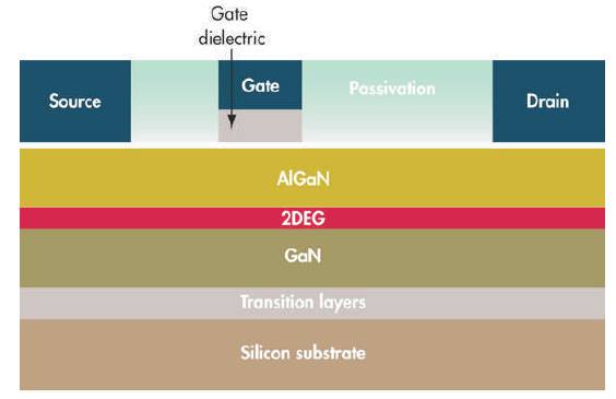
Figure 9. HEMT Structure
The model used in the following simulations is provided by Wolfspeed, a CREE division for power and RF devices. It is possible to obtain the model prior to the registration on the CREE company website. The device under test is the HEMT CGH09120F made in GaN, especially designed for power applications.
The model includes the effect of the temperature and other parasite effects like the “parasite MESFET” (Marani & Perri, 2015).
The first objective is observing the proprieties, non-ideal characteristic, and the side effects of this device, starting from I-V characteristics. The circuit test and the results are shown in Figures 10 and 11, respectively.
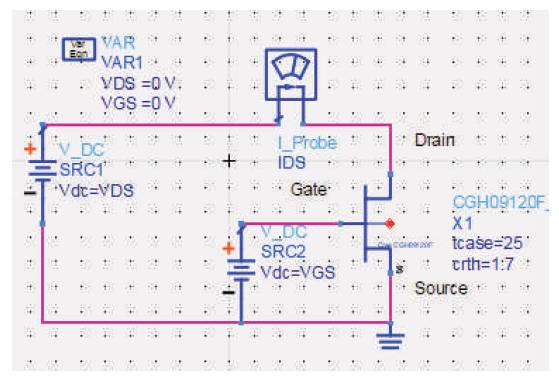
Figure 10. Characteristics Test Bench

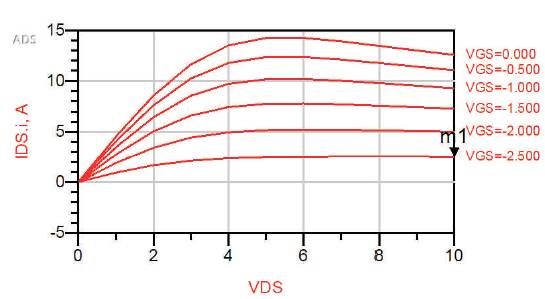
Figure 11. I -V Characteristics
It is important to observe less steep slope with respect to the MESFET simulation at higher value of the gate-source voltage, though the conditions of work are different and this comparison has a simply qualitative relevance. This less slope is caused by the parasite MESFET (Marani & Perri, 2015), a condition that is verified when the layer is not totally empty.
Another important characteristic is the negative slope for higher value of VGS called “negative differential resistance”. It is a side effect of the temperature due to the power dissipation in the device, as shown in Figure 11, where the current is in ampere, VDS in Volt and therefore the power in the circuit has the value of Watt.
HEMTs are especially used in output stages like class A, B, AB, and E-F output stage. The behaviour of the HEMT CGH09120F is used as voltage follower, whose circuit is shown in Figure 12.
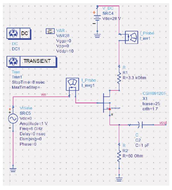
Figure 12. HEMT as Voltage Follower
As shown in Figures 13 and 14, the circuit presents problem at a frequency of 2.5 GHz because output is greater than the input.
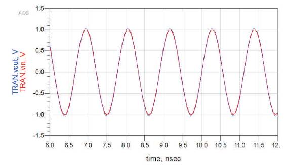
Figure 13. Response at 1 GHz
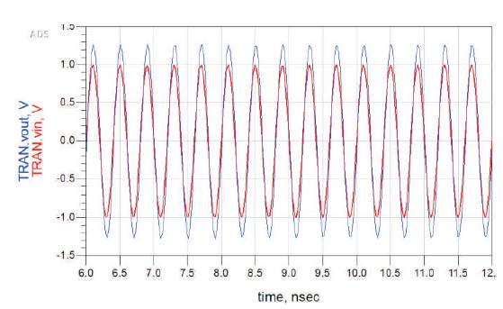
Figure 14. Response at 2.5 GHz
A better configuration for a voltage follower should require an active load on the source, that introduces high impedance and a better current reference but with higher costs.
Figures 15 and 16 show the signals at 5 and 6 GHz, respectively. In the first case the output is higher respect to the input, while in Figure 16, the high attenuation of the signal is obtained. In particular, the drain current decreases if the frequency increases without any possibility to control the gain.
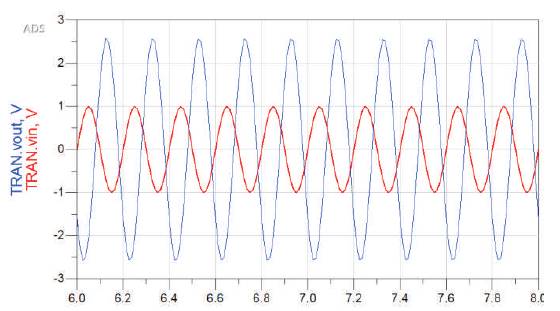
Figure 15. Response at 5 GHz
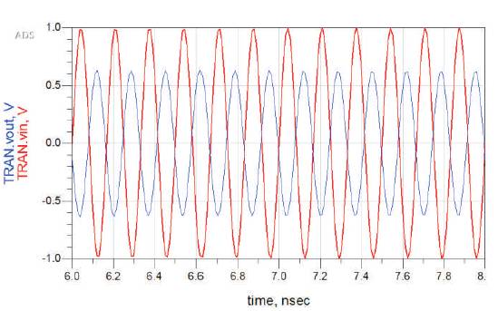
Figure 16. Response at 6 GHz
Figure 17 shows the TFET structure (Mamidala et al., 2016), whose analysis is made by the MIT TFET Model (Sajjad et al., 2017), which includes the non-linearity effects such as the TAT (Trap Assisted Tunnelling). This device improves the performance of low power digital circuits respect to those utilizing MOSFET devices because TFET can achieve higher drain current with smaller gate voltages. The basic principle of this device (Mamidala et al., 2016) is the tunnel effect (Perri, 2016; Marani & Perri, 2015), i.e. the presence of electrons with a certain energy E over a potential barrier with a higher energy is shown in Figure 18.
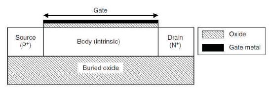
Figure 17. TFET Structure
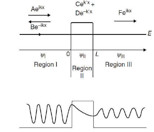
Figure 18. Tunnel Effect Illustration
To obtain this energy situation, it is necessary to introduce a p-i-n (p-type, intrinsic, n-type) structure, as shown in Figure 19, in which the green dot on the channel represents the trap states. The band-diagram assumes an appropriate configuration for the tunnel effect which needs a boost to achieve a useful result. With a no-bias condition of gate, majority carriers of channel see an high potential barrier and the drain current is equal to the reverse-biased leakage typical in p-i-n structures. With a positive gate bias, the energy band in the channel region decreases with the formation of an inversion layer of electrons extended from the drain to the source. Finally, increasing the positive gate bias, the Fermi levels decrease under the drain and the new inversion channel is formed. This condition leads to the creation of a tunnel path for the electrons, if the “windows” in the sourcechannel junction is large enough (Perri 2016; Marani & Perri, 2015). In a TFET, the electrons can pass though the source-channel junction with a lower energy and lower subthreshold swing with respect to the conventional MOSFET.
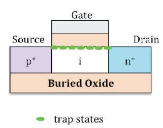
Figure 19. MIT TFET Structure (Sajjad et al., 2017)
In Figure 20, the simulated trans-characteristics of TFET under test is reported and utilizing it in the software (KEYSIGHT technologies, 2016), the MIT TFET model has been proposed in (Sajjad et al., 2017).
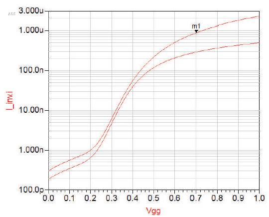
Figure 20. Simulated Trans-characteristics in Logarithmic Scale
As example, a TFET inverter (Figure 21) is studied for low power and high performances in logic circuits. In the same condition of work, a simulated MOSFET as inverter with always Agilent ADS 2016 (KEYSIGHT technologies, 2016), in order to compare them.
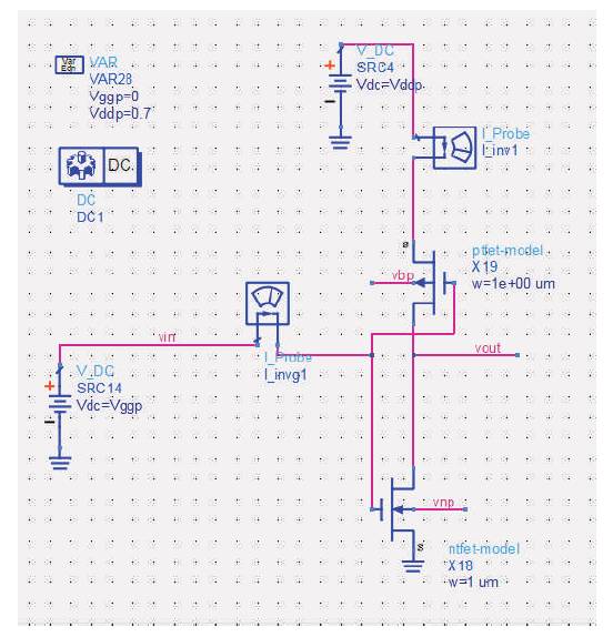
Figure 21. TFET Inverter
The DC characteristics are plotted in Figures 22 and 23, respectively.
It is important to observe the difference in the x-axis. In same condition of work, the vertical characteristic is at 0.35 V and in the MOSFET is at 0.8 V. This has a consequence on the amplitude of the input signal required to indicate a 0 or a1 logic.
With lower amplitude voltage, it is possible to go fast and consume less because the rise and fall time required are lower than in MOSFET application.
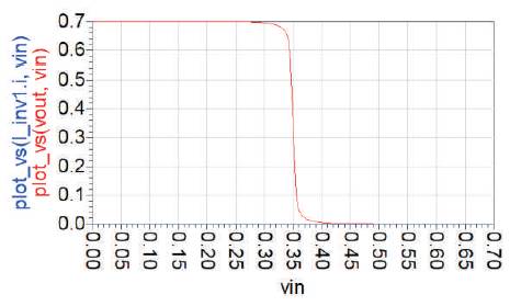
Figure 22. Characterists of TFET Inverter
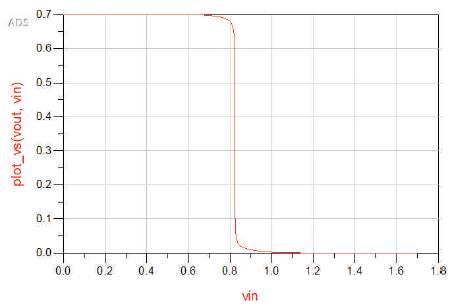
Figure 23. CMOS Inverter Characteristics
It has influence on the noise margin (Figure 24), first the bottom level is equal to zero like CMOS technology, second, a shifted characteristic leads to higher noise margin that reduces the probability of error in read process.
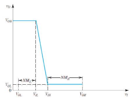
Figure 24. Ideal Representation for Noise Margin
Then the circuit of Figure 25, having a custom digital signal in input is studied. The output, reported in Figure 26 presents an overshoot (Figure 27) and delay propagation.
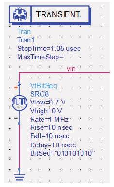
Figure 25. Input Signal Set-up
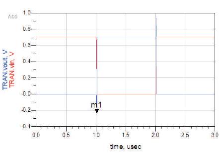
Figure 26. Response of the Circuit
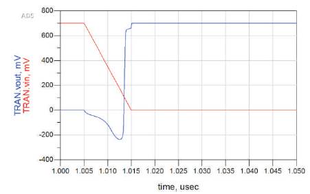
Figure 27. Focus on the Overshoot
A comparison with a MOS inverter (Figure 28) shows that at 100 MHz, there are problems on the lower level of the output as shown in Figure 29. This situation is critical in the presence of electromagnetic interference or another type of disturbance, because a 0 logic can be confused as 1 logic. It is very important that the digital signal rests at 0 or 1 for a specific range of time to allow at the successive device/logic gate to read correctly the digital value.
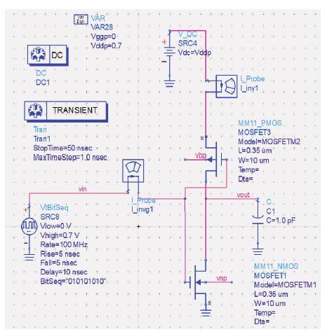
Figure 28. CMOS Inverter
Figure 29. 100 MHz Input Red, Output Response in Blue
Finally, an AND gate based on TFET is designed as shown in Figure 30. The obtained results illustrated in Figure 31, allow us to say that TFET is perfectly suitable for lowstandby- power logic and low-power applications, which are functioning at moderate frequencies.
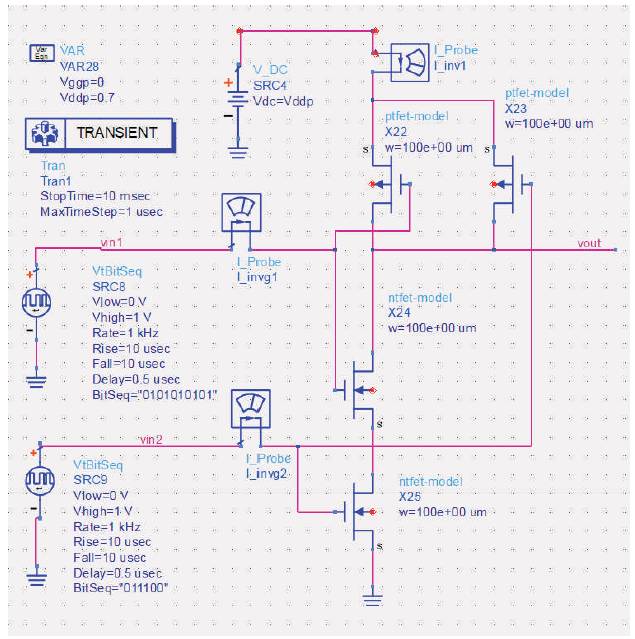
Figure 30. AND Gate with TFET
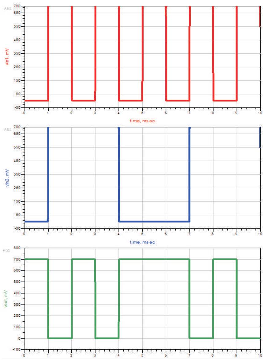
Figure 31. Red: Input 1, Blue: Input 2, Green: Output of AND Gate
In this paper, a comparison among heterostructure devices have been presented. Due to the improvement of modern growth technologies, heterostructure devices are currently used in many electronic applications and the relative models, to employ in circuital simulators, are studied.
MESFET and HEMT present similar characteristic but the second is a little more difficult to use. Both devices present a very good behaviour at high frequency, where their characteristic degrades less in high-signal mode of operation with respect to the equivalent homojunctions.
HEMT is more expensive and for this reason, it is used at output stage in amplifiers in class E-F, designed to have one only device in the circuit. For example, an amplifier in class A with an active load on the source requires two or more HEMTs to obtain the current mirror.
Another technology like CMOS technology cannot guarantee the same performance if used in combination with MESFET or HEMT. On the other side, MESFET is a good alternative as current mirror.
For logic applications, even MESFET and HEMT can be considered because the high electron mobility had made possible the design of high frequency circuits.
Currently, TFET devices seem to be the best solution in logic circuit design. As shown in these simulations, they can work at the same frequency of CMOS circuit, but with different advantages like a better noise margin or lesser voltages to work.
Nowadays, the continuous need to have littler and faster consumer devices, such as laptops, smart-phones, cameras, and so on, drive companies to develop smaller and smaller electronic components. This is the reason why we are studying a new kind of technology, based on molecular devices, which seems to satisfy the market demand and the need to scaling all the electronic components. (Marani and Perri, 2014, 2016a, 2016b, 2016c, 2017).