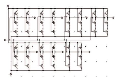
Figure 1. DFAL-TIQ Comparator
A novel Diode Free Adiabatic Logic (DFAL) based Threshold Inverter Quantizer (TIQ) is suggested in this work for implementing a 3-bit Flash type Analog to Digital Converter (FADC). For appropriate implementation of such TIQ, there is a necessity of rehabilitated reference voltage for each of the comparator and this task is accomplished methodically by sizing the transistors of the TIQ comparators. The suggested work is carried out with TSMC 65 nm Technology on Cadence- Virtuoso-IC616 version. The average power dissipation by the proposed FADC simulated at 1.2 V and for 1fF capacitive load is 5.5 μW, which is 66 % less than that of the power consumed by CMOS-TIQ based FADC at 100 Hz.
The high speed handheld devices operated on battery utilizes Analog to Digital Converter (ADC) as a part of system instead of a distinct circuit used for data translation. This use of ADC requires minimum power dissipation. There are some tactics used to reduce the power, such as reducing supply voltage and switching activity. These tactics are not sufficient enough to meet modern day's power requirement. Due to this reason most of the designers have focused on adiabatic logic-based circuit development to accomplish the desired objective (Cho and Gray, 1994; Yoo, 2003; Yoo et al., 2001;Teichmann, 2012).
The proposed work is projected to implement a Flash type ADC using Diode Free Adiabatic Logic (DFAL) based Threshold Inverter Quantizer (TIQ) comparator instead of traditional CMOS logic.
Most dynamic component in the Flash type ADC construction is a comparator. The comparator architecture for the flash type ADC is suggested by using assorted comparators, such as differential-amplifier latch, auto-zeroed sequentially sampled type, dynamic type, Threshold Inverter Quantizer (TIQ), and Quantum- Voltage (QV). Faster conversion rate is attained by the TIQ based comparator design (Upadhyay et al., 2013; Kaess et al., 1997; Kanan et al., 1999).
Conventional CMOS-TIQ comparator grieves with switching power dissipation; a way for reducing power dissipation in TIQ comparator is projected by using adiabatic logic, which uses the Diode Free Adiabatic Logic as its base for effective reduction of power consumption (Upadhyay et al., 2013; Kanan et al., 1999; Kaess et al., 1997). The required comparator for 3-bit Flash ADC is depicted in Figure 1.
Figure 1. DFAL-TIQ Comparator
In the DFAL-TIQ comparator, each of the inverter is comprised of two identical stages, viz., first stage is to provide the desired threshold voltage level and the second stage is the gain booster stage, which is used to maintain the same DC threshold level and to retain the linearity of DFAL-TIQ in poise.
The proposed comparator requires seven stages of DFAL inverter (2no of bit -1 = 23 -1 = 7) with varying threshold of each inverter. The variation of the threshold voltage in the inverter will ensure the faithful binary output production at each stage. The proposed DFAL-TIQ is simulated using Cadence-Virtuoso-IC616 on TSMC 65 nm technology, and the simulation results for the transient sweep analysis and DC sweep analysis are as depicted in Figure 2 and Figure 3 respectively.
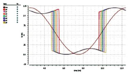
Figure 2. DFAL-TIQ Transient Sweep Analysis
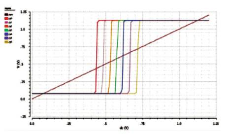
Figure 3. DFAL-TIQ DC Sweep Analysis
The variation of the threshold voltages for each stage of DFAL - inverter can be easily observed in Figure 2 and Figure 3. During transient analysis, the input analog signal of frequency 100 Hz and 1.2 Vpp is applied and for DC sweep analysis, the input voltage is varied in linear steps from 0 V to 1.2 V.
The output of the DFAL-TIQ comparator is the thermometric code format. Therefore to convert this format into its equivalent binary code, the Thermometric to Binary Code Converter (TM2B) is employed. The unpretentious method to implement Thermometric to Binary code converter is by means of a binary encoded Read Only Memory (ROM) (Kanan et al., 1999). Alternatively, the converter can also be comprehended by Wallace tree (Lee et al., 2002). In advanced stages of development, fat tree converter was also utilized for the realization of code converter (Sail and Vesterbacka, 2004).
The presented effort utilizes a converter implemented using 2:1 multiplexer as elementary component, as it has numerous advantages, such as low circuit complexity and low power consumption. Schematic implementation plan for a 7 to 3-line converter is revealed in Figure 4.
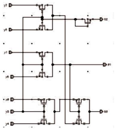
Figure 4. Mux based Thermometric to Binary Code Converter
The schematic of the TM2B converter is arranged in such a way that is should satisfy all the eight conditions of Table 1. Each row in the Table indicates that a binding input thermometric code is obtained from the output of comparator stage and its corresponding 3-bit binary output, which in turn will be considered as the output of the Flash ADC.
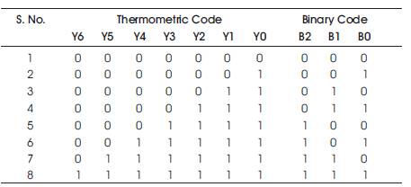
Table 1. Thermometric to Binary Conversion Truth-Table
Schematic diagram for anticipated Flash ADC is depicted in Figure 5, which is build using two-stage architecture. First stage comprises of the DFAL-TIQ comparator which also includes the gain booster stage. In the second stage, the code converter is cascaded with the comparator stage to furnish a whole ADC.
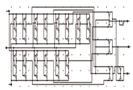
Figure 5. Schematic of DFAL-TIQ based Flash ADC
The proposed flash ADC is simulated using simulated using Cadence-Virtuoso-IC616 on TSMC 65 nm technology, and the simulation results for the transient sweep analysis and DC sweep analysis are as portrayed in Figures 6 and 7, respectively.
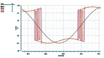
Figure 6. Transient Response of Flash ADC
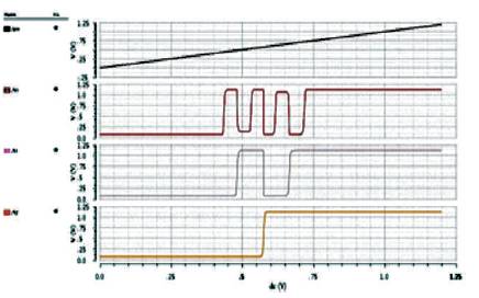
Figure 7. DC Response of Flash ADC
From these response plots, it is deceptive that input Vin is varied from 0 V to 1.2 V in linear steps, and binary output bits b2, b1 and b0 are observed; which sequentially appears as 111, 110, 101, 100, 011, 010, 001, 000 at a specific time interval. This time interval is decided by the systematic variation of the widths and lengths of the transistors used in the design.
Transient analysis of the proposed circuit is carried out at various input frequency signals in order to acquire a relative analysis of power dissipation at 1.2 V at different frequencies as shown in Table 2.
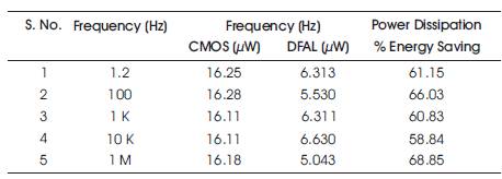
Table 2. Power Dissipation Comparison of CMOS based and DFAL based ADC as a Function of Frequency Variation
Diode Free Adiabatic Logic (DFAL) TIQ is a novel adiabatic logic family TIQ for Flash type ADC. The simulation results and relative performance assessment revealed that power consumption in the DFAL logic family are considerably lower than the CMOS family; thus, the proposed DFAL family outperforms and provides almost 63% of energy savings.