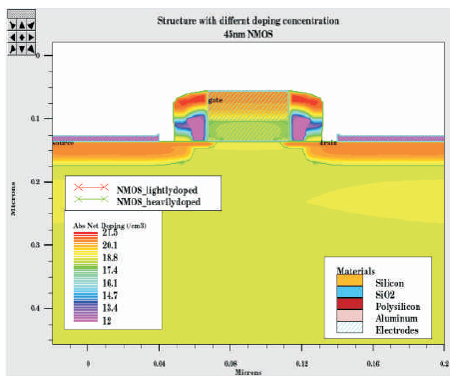
Figure 1. Structure of NMOS Device (LD and HD)
This paper explores the impact of lightly doped (LD) and heavily doped (HD) substrates on a Metal Oxide Semiconductor Field Effect Transistor (MOSFET) with 40 nm Gate length. The influence of varying the p-type substrate doping 15 18 -3 concentration (from 10 to 10 cm ) is investigated in terms of the drain current, substrate current, sub-threshold current, on-off current ratio, sub-threshold swing and threshold voltage. The simulation results show that the lightly doped substrate devices with high work-function (wf) gives improved off-state leakage current. It has also been observed that LD devices have high drain current even on low gate oxide thickness. All the simulation and design work have been done in SILVACO TCAD software.
Earlier, the heavily doped substrates were preferred due to its low sensitivity to Latch-up problem, low soft error rate and low shunt to substrate resistance. As the resistance is decreased, Metal-Oxide-Semiconductor Field-Effect Transistor (MOSFET) must achieve a higher substrate current to undergo MOSFET snapback which is the major drawback of heavily doped (HD) substrate devices. There comes an idea to use lightly doped (LD) substrates instead of heavily doped which have better characteristics. Lightly doped substrates provide low substrate capacitance, good noise isolation with reduced cost. Lowering the collector leads to increase in unity power gain cut-off frequency. The ESD robustness of lightly doped substrates is higher than the heavily doped substrates. It also has low snapback voltage which is the best characteristic of lightly doped over heavily doped devices.This paper reveals that lightly doped substrate is much better in comparison to heavily doped substrate in terms of noise immunity (Yang et al., 2006).
The Impact Ionization occurs in the MOSFETs because high electric fields cause an impact which generates a hole-electron pair. The electrons flow out of the drain and the holes flow into the substrate causing a substrate current to flow. The impact ionization is the physical mechanism for the generation of substrate current. As the channel length of MOSFETs is reduced to sub-micrometer range, the electric field near the drain region causes impact ionization at a significant rate. The generated hole current in the MOSFET flows into the substrate as substrate current. The substrate current can cause problems such as latch-up, shift of threshold voltage, and degradation of trans-conductance in short channel devices. The substrate current also contributes to output conductance in the saturation region and breakdown characteristics (International technology roadmap for semiconductor, 2011).
A 45 nm NMOS device has been designed using lightly doped substrate having doping concentration of 5e15 cm , and heavily doped substrate having doping -3 concentration of 5e18cm . The difference in both devices is only the doping concentration but it results in variation in various parameters. The physical gate length is considered as 40 nm. The structure of NMOS device is shown in Figure 1.
Figure 1. Structure of NMOS Device (LD and HD)
Figure 1 shows the structure of NMOS device with lightly and heavily doped substrate which has been designed in ATHENA of SILVACO software and simulated using ATLAS of SILVACO software.
The drain current model is as follows:
where the drain-source voltage is replaced by the channel voltage. The equation can be integrated both sides from the source to drain, left side from 0 to the gate length, L, and right side from 0 to the drain-source voltage, VDS
The drain current, I , is constant so that integration results D become,
The drain current first increases linearly with the applied drain-to-source voltage (V ), but then reaches a DS maximum value. According to equation (3) the current would even decrease and eventually become negative. The charge density at the drain end of the channel is zero at that maximum value, and changes sign as the drain current decreases. The charge in the inversion layer also goes to zero and reverses its sign as the holes are accumulated at the interface. However, these holes cannot contribute to the drain current, since the reverse biased p-n diode between the drain and substrate blocks any flow of holes into the drain. Instead, the current reaches its maximum value and maintains that value for higher drain-to-source voltages (Nicollian et al., 1982, Sze, 2003). A depletion layer located at the drain end of the gate accommodates the additional drain-to-source voltage. This behaviour is referred to as drain current saturation. The drain current in saturation region, I is dsat given by:
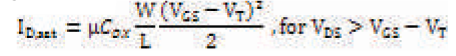
The drain current model explains the drain current versus drain voltage characteristics of a MOSFET, which are normally plotted for different gate-to-source voltages (Amin et al, 2011). The simulated drain voltage characteristics at various drain voltages and gate voltages are shown in Figure 2.
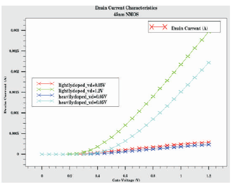
Figure 2. I versus V Plot D GS
Figure 3 shows that maximum drain current is achieved using lightly doped devices. The Negative Channel Metal Oxide Semiconductor (NMOS) device with channel length of 45 nm has been simulated in ATLAS SILVACO (ATLAS Device Simulator; Sachdeva et al., 2017a). By increasing the substrate doping concentration i.e. at higher substrate doping, both the on-current and off- current decreases, but the rate of reduction in the off-current is faster than the on-current in such a way that the ratio of the on-current to off-current becomes very high, at a 15 18 -3 substrate doping concentration from 10 to 10 cm .
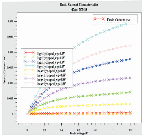
Figure 3. I versus V Plot
If the gate oxide thickness is reduced further, it results in increase in the electric field across the oxide. The high electric field together with low gate oxide thickness, results in tunneling of electrons. This phenomenon occurs from substrate to gate and from gate to substrate, through the gate oxide, resulting in gate oxide tunnelling current. Figures 4 and 5 shows that there is a prominent gate leakage current in heavily doped NMOS device as compared to lightly doped NMOS device (Gupta et al., 2013).
Figure 4. I versus V Plot
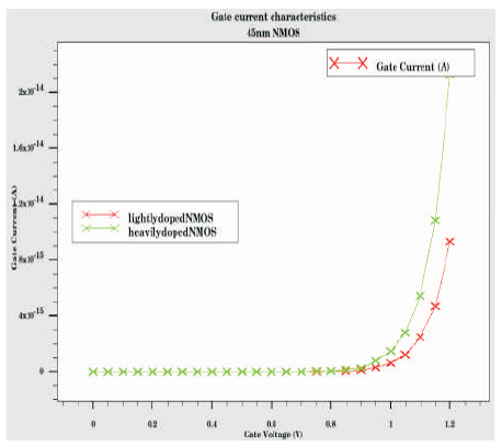
Figure 5. I versus V Plot
The threshold voltage of the MOSFET is dominantly determined by the work function (wf) of the gate material. It is reported that in nanometer scale Field-Effect Transistor (FET) with a thin gate oxide, control of the threshold voltage b y i n c r e a s i n g d e p l e t i o n c h a r g e s h a s ma n y disadvantages, like carrier mobility degradation, large threshold voltage fluctuation due to random dopant distribution and large sub-threshold slope (Kloes et al., 2012, Sachdeva et al., 2017b). The threshold voltage (V ) T depends not only on the gate work functions, but also on the silicon and gate oxide thickness. In order to handle V , T it is important that the gate material should have a variable work function. A key technological challenge for MOSFET is to find gate materials with proper work functions, for the desired threshold voltages. Therefore, a gate electrode with a proper work function, that places its Fermi level close to the middle of the silicon band gap is desired, so that the work function difference between the gate electrode and the near-intrinsic silicon film can be adjusted to optimize the threshold voltages of both n- and p-channel devices in a Complementary metal–oxide– semiconductor (CMOS) circuit (Ch et al., 2015).
Initially, Negative Channel Metal Oxide Semiconductor (NMOS) with heavily doped substrate and lightly doped substrate is simulated with work-function equal to 4.12eV. After simulation, it has been observed that drain current of lightly doped substrate NMOS is more than heavily doped NMOS as shown in Figure 4. But there is an increase in off state leakage current in LD device (Dutta, et al., 2017, Persson et al., 2013). By increasing the work-function of LD device, the off state leakage current can be reduced to 2.580 nA.
Figures 6-8 show that as the work-function of the LD and HD devices increase, the ON current of both the devices also increase, but LD device shows maximum current of 2973 μA.
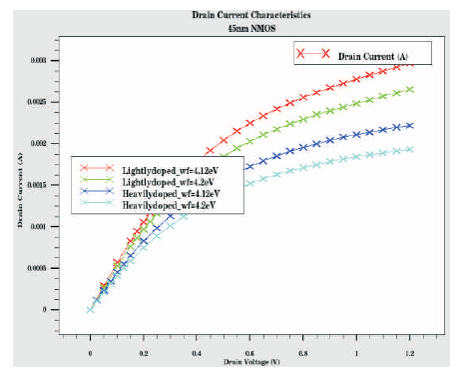
Figure 6. I vs V Plot at wf=4.12eV and wf=4.2eV
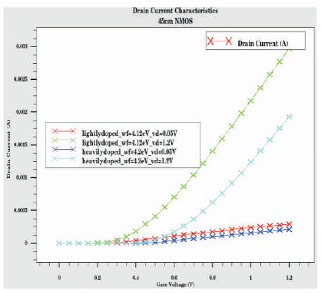
Figure 7. I vs V Plot at wf=4.12eV and wf=4.2eV
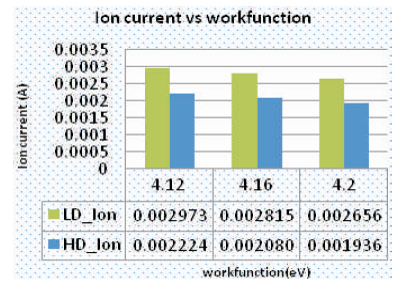
Figure 8. Variation of ON Current with Different Work-functions
The substrate current expression can be derived by integrating the carrier impact ionization coefficient over the velocity-saturated region of the channel.
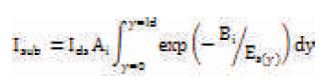
where, A and B are the impact ionization coefficients. i i E (y) is the electric field along the channel direction, y=0 s is at the edge of the velocity-saturation region in the channel and l is the length of the velocity-saturation D region. I is the drain current without consideration of the Ds impact ionization effect (Mehrotra et al., 2013). A pseudo-two-dimensional analysis can find E (y) in the s velocity saturated region. There is an exponential relationship of E (y) versus distance, where E is the s sat critical field for velocity saturation and l is the t characteristic length of the exponentially rising electric field which is given by,
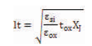
where, t is the gate oxide thickness and X is the ox J drain/source junction depth. ε and ε are the dielectric ox si permittivity of silicon dioxide and silicon, respectively. The above expression (6) can also be expressed in terms of voltage within the saturation region.
After simulation of LD and HD devices, substrate current is noted more in LD device, but it can be reduced by increasing the work-function of the device to 8.277e-07A as shown in Figures 9 and 10.
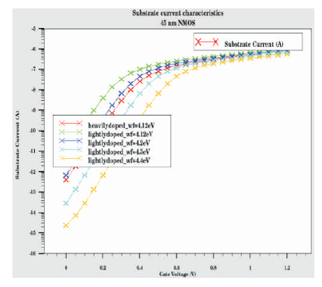
Figure 9. I vs V Plot at different Work-functions
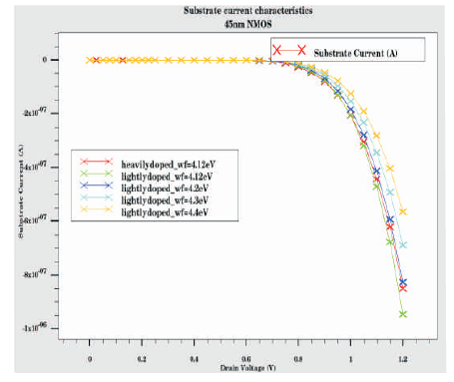
Figure 10. I vs V Plot at Different Work-functions
The gate oxide thickness is scaled from 2 nm to 1 nm. As the gate oxide thickness varies from 2 nm to 1nm, the drain current is more in lightly doped NMOS as compared to heavily doped NMOS as shown in Figure 11.
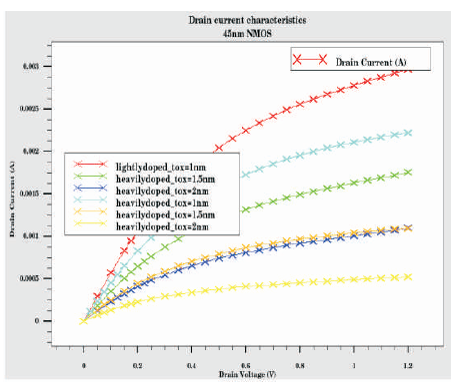
Figure 11. I vs V Plot at Different Gate Oxide Thickness
Figures 12 and 13 show the simulation of ON current for lightly doped and heavily doped devices. The graph shows that as the gate oxide thickness is scaled down, the ON current of heavily doped NMOS decreases but, ON current of lightly doped device increases with decrease in gate oxide thickness as required.
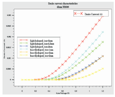
Figure 12. I vs V Plot at Different Gate Oxide Thickness
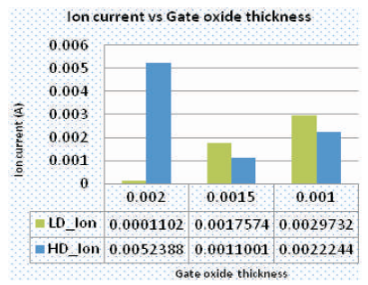
Figure 13. Variation of Ion Current with Gate Oxide Thickness
Figure 14 shows the decrease in threshold voltages (V at tsat V =1.2V and Low Threshold Voltage (V ) at V =0.05V) of DS TL DS lightly doped and heavily doped devices, but lightly doped NMOS has achieved best value of 0.22 V threshold voltage as per International Technology Roadmap for Semiconductors (ITRS) guidelines.
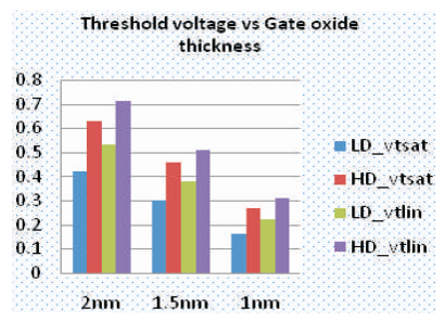
Figure 14. Variation of Threshold Voltages with Gate Oxide Thickness
Figure 15 shows that there is a decrease in subthreshold slope with t in both lightly doped and heavily doped ox devices, but lightly doped device has achieved reduced sub-threshold slope of 72 mV/decade as compared to heavily doped device.
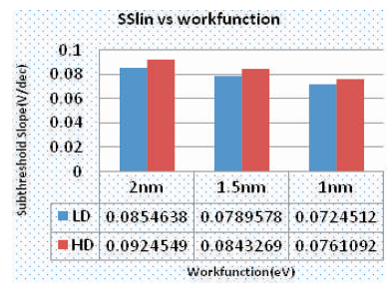
Figure 15. Variation of Subthreshold Slope with Gate Oxide Thickness
Lightly doped and heavily doped MOS devices are virtually fabricated and their characteristics are evaluated for drain current, substrate current, threshold voltage and off current. Lightly doped substrate provides better ON current equal to 2973 μA, better threshold voltage equal to 0.22 V, better off current equal to 2.580 nA, better substrate current equal to 8.277e-07A, better sub-threshold slope equal to 72 mV/decade even at low t in comparison to heavily doped substrate. Substrate ox current is more pronounced in the case of heavily doped substrate, making it less suitable at device level. Also, by increasing the work-function of the gate electrode, off state leakage current can be reduced in lightly doped devices. Therefore, the lightly doped substrate devices provide better substrate noise immunity and devices fabricated on lightly doped substrate provide better drain characteristics than heavily doped substrate devices.