Table 1. Timing Requirements of RGMII v2.0 Interface
In this paper, the problem of reducing difference between rise and fall delays (output delay skew) of Input/Outpuut (I/O) cells and duty cycle enhancement to meet 2.5 V Reduced Gigabit Media Independent Interface (RGMII) 2.0 interface I/Os timing requirements at Gigabit Ethernet 125 MHz clock speed was investigated and analyzed. Stacked I/O design specifics (reference voltages and their instability) were considered for example design of 2.5 V I/Os in 28 nm technology with 1.8V dual-gate-oxide (dgo) transistors (Yoshida, 2017 ). Testbench for test I/O bank Layout Parasitic Extraction (LPE) netlist spice simulations was created in Cadence Virtuoso design environment for I/O rise/fall delays and duty cycle evaluation at bank-level including package Resistor-Inductor-Capacitor (R-L-C) and T-line models, and worst data toggle patterns were used to take simultaneously switching effects into account. Method for connecting decoupling capacitors to reference voltages was used to achieve reduced voltage noise, adjusted rise/fall delays, reduced skew, and output signal stabilized for both single I/O and I/O bank. Analysis was carried out for various values of decoupling capacitors to calculate appropriate one and meet the given RGMII specification timing requirements.
Reduced Gigabit Media Independent Interface (RGMII) interface (Gigabit Ethernet) (Chen et al., 2003) is widely used in Next Experience (NXP) application processor products (Ingels and Steyaert, 1997) at 1.5/1.8/2.5/3.3 V voltages and 125 MHz clock frequency. Output rise/fall delay skew (TskewT: +/-500 ps) and duty cycle (Duty_G: 50+/-5%) timing parameters of RGMII v2.0 interface are the design targets, which are shown in Table 1.
Table 1. Timing Requirements of RGMII v2.0 Interface
Usually during System on a Chip (SoC) design, limited duty cycle and output delay skew budgets are provided as Input/Output(I/O)s. As an example, consider the following design targets: +/- 2.5% budget for duty cycle (out of total 5%), and 150 ps (out of total 500 ps) budget for output delay skew. Rest of the timing budgets are usually given mainly for Phase Locked Loop (PLL) and Core Logic contribution. In typical design flow, Static Timing Analysis (STA) for RGMII interface is closed using I/O timing numbers from liberty files (.lib) of I/O library.
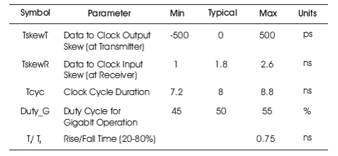
In this example design, RGMII I/Os were simulated at the following conditions: Layout Parasitic Extraction (LPE) netlist across Process-Voltage-Temperature (PVT) corners, with typical R-L-C package parameters (FlipChip or WireBond packages can be used), and simplified board model (emulated with T-line). Figure 1 shows the block diagram for I/O simulation testbench (defined by RGMII 2.0 standard) with T-line.
Figure 1. Measurement Circuit for IO Skew/Duty Cycle with T-line
RGMII/Gigabit Ethernet interface development (including I/O design) is one of the regular development tasks in industry (NXP Semiconductors). If only 1.8 V dual-gate- Oxide (DGO) Metal-Oxide-Semiconductor (MOS) transistors are available for design, typically 2.5 V I/Os are developed in cascoded/stacked configuration of I/O cell blocks (Singh, 1998). This architecture is also valid for 2.5 V RGMII I/Os in 28 nm technologies (Yoshida, 2017), and this paper focuses on the analysis of a typical architecture of RGMII I/O blocks. To meet transistor reliability rules and avoid device voltage overstress, stacked I/O design configuration requires reference/bias voltages (REFp, REFn, shown in Figure 2) and a separate circuit for their generation (reference generator, or REF_GEN). REF_GEN circuit can be designed as separate core macro cell, placed outside of pad ring. It can also be placed once for each RGMII I/O bank.
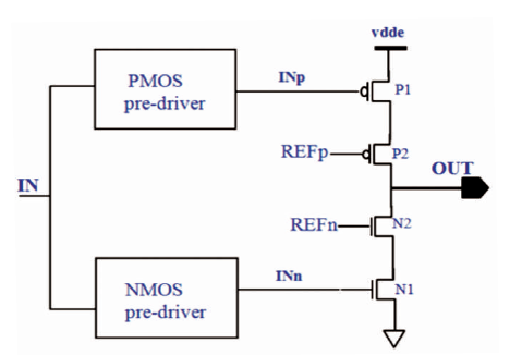
Figure 2. Basic Architecture of Stacked I/O
Usually reference voltages in stacked I/Os are very unstable, especially at high frequency, that greatly degrades I/O timing parameters like output rise/fall delay skew and duty cycle, especially as a result of bank-level Simultaneously Switching Outputs (SSO) effect (Jou et al., 2001; Tang, and Friedman, 2002), if no special design techniques are used.
In this example, how a design methodology works to meet RGMII specification timing parameters is demonstrated. For I/O skew and duty cycle analysis, it is very important to run bank-level simulations with worst data switching patterns. The representative test bank for RGMII interface included bias/reference supply generator (REF_GEN), special level shifter/filler cell to propagate reference signals from core to pad ring and 6 I/O signal/data cells.
Test bank simulations were carried out with the following three different patterns or “data switching activities”:
I/O design timing analysis, and timing enhancement methodology are the objectives of this study, which are detailed as follows:
The block diagram of simulation testbench for RGMII I/O bank is shown in Figure 3, and reference voltages waveforms without decaps are shown in Figure 4.
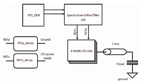
Figure 3. Block Diagram of Simulation Testbench for RGMII I/O Bank
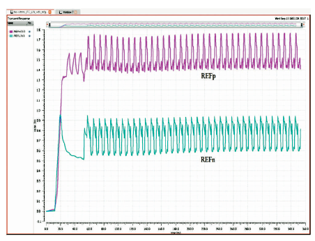
Figure 4. Reference Voltage Waveforms without Decaps
The following rise/fall times, delay and duty cycle simulation numbers are given for this specific testbench example in this paper.
Table 2 presents the results for 'even' data switching pattern without any decoupling capacitors. Values of delay skew and duty cycle does not satisfy I/O design targets.
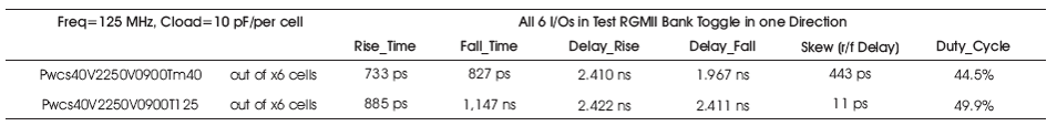
Table 2. Timing Simulation Data of RGMII I/O Bank without Decaps, Even Pattern
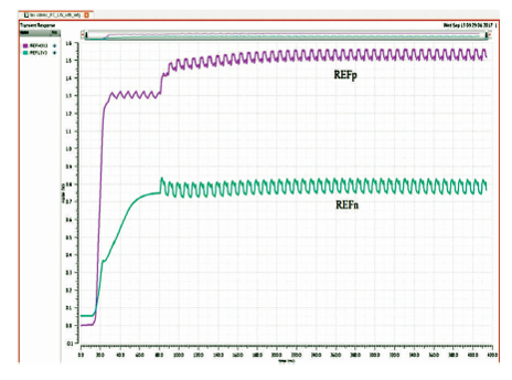
Figure 5. Reference Voltage Waveforms with Decaps
It is clearly visible that reference voltage curves in Figure 5 are much more stabilized and hence I/O has better timing in terms of duty cycle and skew. Decaps to reference voltages may be placed partly into filler cells in Input/Output (IO) ring and partly into the chip core area (providing routing resistance requirements from core decap to IO ring).
In Tables 3, 4, and 5, simulation results of RGMII I/O duty cycle, rise/fall time, delays and skew at the worst PVT conditions for timing and different data switching activities are given for the specific example testbench.
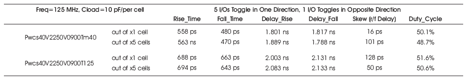
Table 3. Timing Simulation Data of RGMII I/O Bank with Decaps, Odd Pattern

Table 4. Timing Simulation Data of RGMII I/O Bank with Decaps, Even Pattern
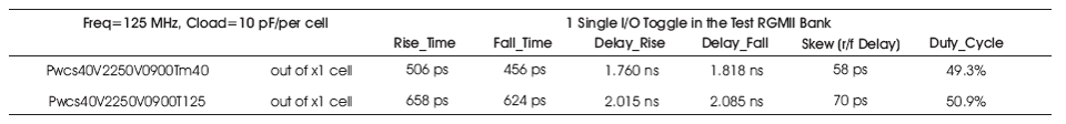
Table 5. Timing Simulation Data of RGMII I/O Bank with Decaps, 1 Single I/O Toggle
In 28 nm technology with 1.8 V dgo MOS transistors, 2.5 V RGMIII/O circuits are usually built on stacked design architecture with REFp/REFn reference voltages used for reliability reasons. Single I/O cell circuit design optimization itself for timing may not be enough for every circumstances to meet given interface delay skew and duty cycle requirements. Unstable reference voltages have big impact on I/O timing and degrade performance at bank-level toggling if no special design methodologies are used. Test I/O bank-level simulations with full RGMII interface environment, such as worst data toggle switching patterns, typical R-L-C package and Tline models proved that decoupling capacitors placement on I/O reference voltages is a very efficient technique to stabilize them and hence meet the duty cycle and skew targets assumed in this design example. Reference voltage decaps can be placed partly into filler cells in IO ring and partly in the chip core area. This design approach was successfully used in NXP application processors.