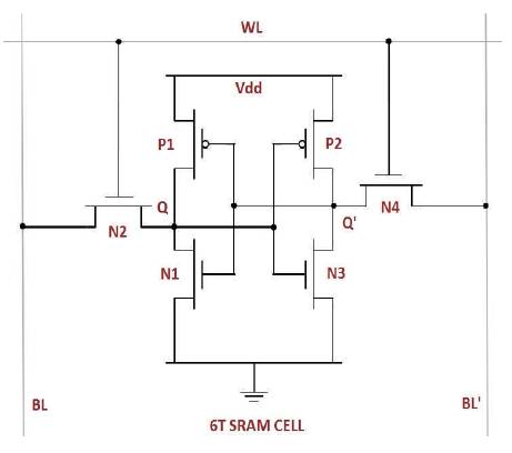
Figure 1. A basic SRAM Cell
In this paper, the authors have designed a 1bit and 8bit SRAM (Static Random Access Memory) cell using pulsed latch circuit in 45 nm, 90 nm, and 180 nm CMOS technologies with 1.0 V,1.2 V and 1.8 V power supply, respectively. The memory cell has become a basic building element in the field of electronic circuit design. The memory cell consists of wide range of applications. It has good specifications due to its large storage capacity, lower access time, and high speed. SRAM cell has become the topic of research due to its increase demand in laptops, memory cards, and in mobile applications for both on-chip and off-chip memories. So, it is very necessary to reduce its power and delay so as to increase its speed. The main aim of this design approach is to reduce power and delay of the SRAM cell. In this design approach, the two NMOS access transistors are replaced by pulsed latch circuit. The pulsed latch circuit consists of 7 transistors in which it has two differential data inputs and a clock signal, also it has two differential data outputs. In this design approach, it is observed that the power and delay is reduced as compared to that of the conventional SRAM cell design. The proposed design has been designed in S-Edit, simulated using T-Spice and their waveform can be viewed in W-Edit. The proposed design has been carried out in Tanner tool v16.0.
Memory structures have become an important part of modern VLSI systems. SRAM (Static Random Access Memory) cell retains data bits in its memory as long as power is being supplied. Unlike DRAM (Dynamic Random Access Memory) cell which stores bits in cells consisting of a capacitor and a transistor. SRAM is much faster than DRAM because it does not have to be periodically refreshed [1].
SRAM cell has large storage density, small access time, high operating speed, and lower power dissipation. There are many applications of SRAM cell. SRAM cell has become the latest topic of research due to its huge demand in mobile applications, in laptops and in IC memory cards ([4],[12],[15]).
SRAM is a bistable latching circuit with two NMOS access transistors. SRAM stores binary logic '0' and '1' bits. A basic 1bit SRAM cell has 6 transistors which consist of two PMOS and four NMOS transistors. A basic SRAM cell is shown in Figure 1. In this figure, transistors P1, P2, N1 and N3 act as a storage element and transistors N2 and N4 are the two access transistors. Word Line (WL) is connected to the access transistors at their gate terminals, which is used to select the cell. Source/Drain terminals are connected to the Bit Lines (BL and BL'),these lines are used to perform the read and write operations on the cell ([2],[6],[9]).
Figure 1. A basic SRAM Cell
Since the operating speed of SRAM cell is very high and also it has small access time, so it is very necessary that speed of the SRAM should be high. In order to achieve high operating speed, delay and power consumption of SRAM should be less [10].
So, in this paper we proposed a method in which we design SRAM cell with pulsed latch circuit and compare their results.
This paper organized as follows: Section 1 gives brief description of design approach of SRAM cell using Pulsed Latch circuit. Section 2 presents the design and waveform of SRAM cell in different CMOS technologies. Section 3 presents the design and waveform of SRAM cell using pulsed latch in different technologies. Section 4 shows comparision results.
In this paper, SRAM cell is designed using pulsed latch circuit. The two NMOS access transistors are replaced by pulsed latch circuit. Here, pulsed latch circuit is used to reduce delay and power of the pulsed latch circuit, because the main aim of the pulsed latch circuit is to reduce delay. In this paper, the authors have used SSASPL (Static Differential Sense Amp Shared Pulse Latch). The SSASPL is the smallest latch which consist of 7 transistors. The SSASPL consists of 2 cross coupled inverters and 3 NMOS transistors. This pulsed latch circuit consumes less power and delay because it has a single transistor driven by the pulsed clock signal ([3], [5], [7],[13], [16]).
The schematic of the SSASPL is shown in Figure 2. The SSASPL updates its data with three NMOS transistors and the two cross coupled inverters act as storage element. It consist of two differential data inputs D and Db and a pulsed clock signal and two differential data outputs Q and Qb. When the pulsed clock signal is high it updates the data. The value of pull-down current of the three NMOS transistors must be large than the value of pull-up current of the PMOS transistors in the cross coupled inverters ([3], [8], [10], [11], [14]).
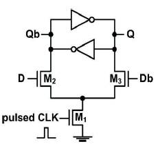
Figure 2. Schematic of the SSASPL
A 1bit SRAM cell is the basic 6T SRAM cell which consist of 2 PMOS transistors and 4 NMOS transistors. The schematic of 1bit SRAM cell is shown in Figure 3. The SRAM cell works according to the value of wordline, when the value of wordline is one then only it writes the value in SRAM cell. The schematic of SRAM cell which is shown in Figure 3(a) is in 45 nm technology.
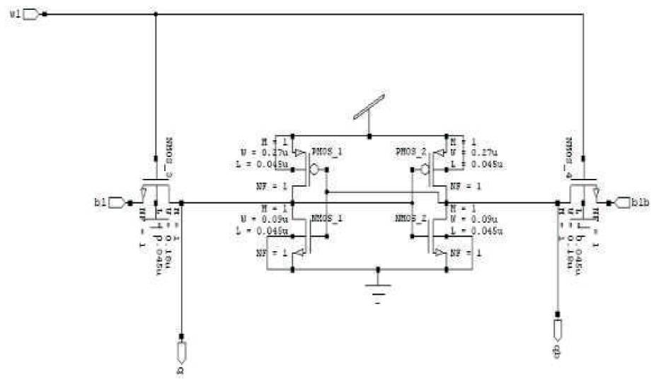
Figure 3(a). The Schematic of 1bit SRAM Cell
The waveform of 1bit SRAM cell in three different technologies that is 45 nm, 90 nm and 180 nm technology are shown in Figure 3(b), 3(c), and 3(d) respectively.
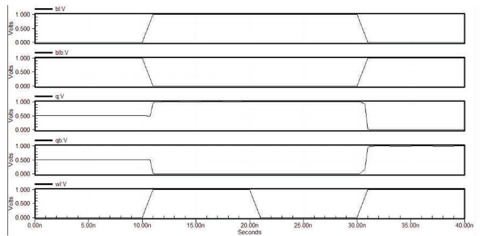
Figure 3(b). Waveform of 1 bit SRAM in 45 nm Technology

Figure 3( c). Waveform of 1 bit SRAM Cell in 90 nm T echnology
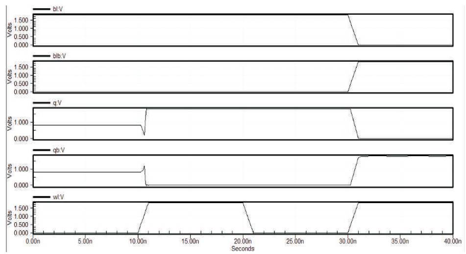
Figure 3(d). Waveform of a 1 bit SRAM Cell in 180 nm Technology
The 8 bit SRAM cell consist of eight 1 bit SRAM cell. Each SRAM cell consist of its own input and output lines. It has two data inputs and two data outputs, each cell is connected to a common word line signal. The schematic of 8 bit SRAM cell is shown in Figure 4(a).
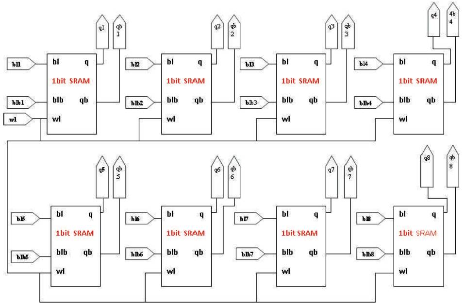
Figure 4(a). Schematic of 8 bit SRAM Cell
The schematic of 8bit SRAM cell which is shown in Figure 4(a) is in 45 nm technology. The waveform of 8 bit SRAM cell in three different technologies that is 45 nm, 90 nm and 180 nm are shown in Figure 4 (b), 4(c), and 4(d) respectively.
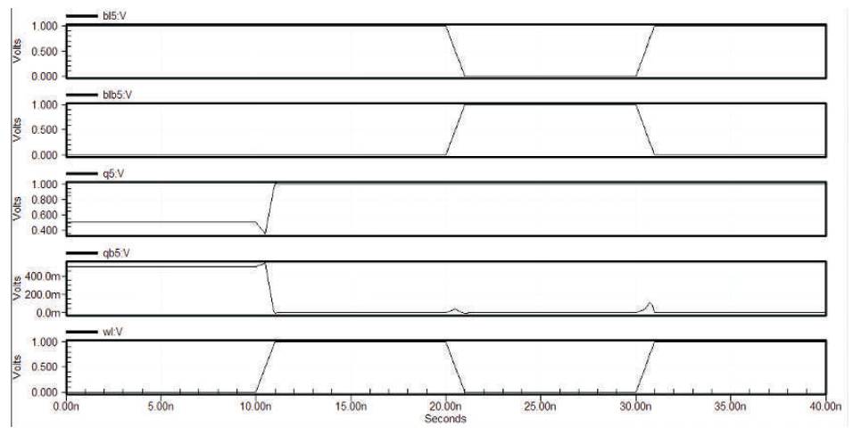
Figure 4(b). Waveform of 8 bit SRAM Cell in 45 nm Technology
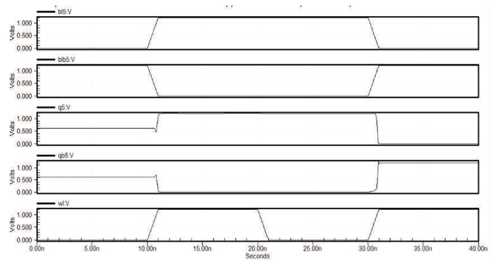
Figure 4( c). Waveform of 8 bit SRAM Cell in 90 nm Technology
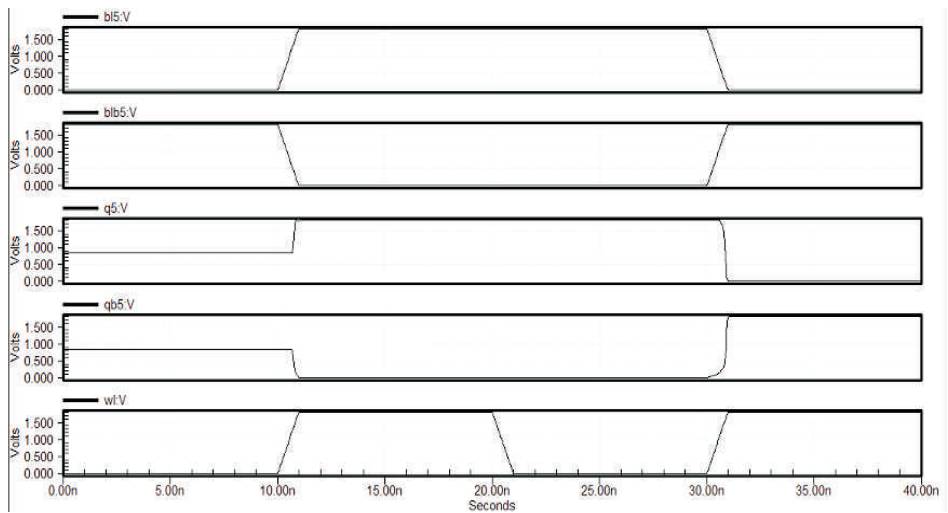
Figure 4(d). Waveform of 8 bit SRAM Cell in 180 nm Technology
The 1bit SRAM cell using pulsed latch consist of 11 transistors, in which 7 transistors are used to design a pulsed latch circuit and remaining transistors are used to make two cross-coupled transistors. Here, pulsed latch circuit is used in order to reduce delay and power of the SRAM cell. The schematic diagram of 1 bit SRAM cell using pulsed latch is shown in Figure 5(a). The cell has two inputs bl and blb with a pulsed clk signal and two outputs q and qb.
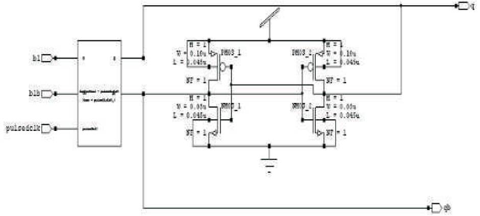
Figure 5(a). Schematic of 1bit SRAM Cell using Pulsed Latch
The waveform of 1bit of SRAM cell using pulsed latch in three different technologies that is 45 nm, 90 nm and 180 nm are shown in Figure 5(b), 5(c), and 5(d) respectively.
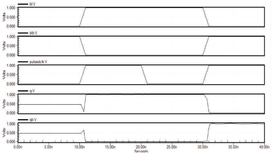
Figure 5(b). Waveform of 1bit SRAM Cell using Pulsed Latch in 45 nm Technology
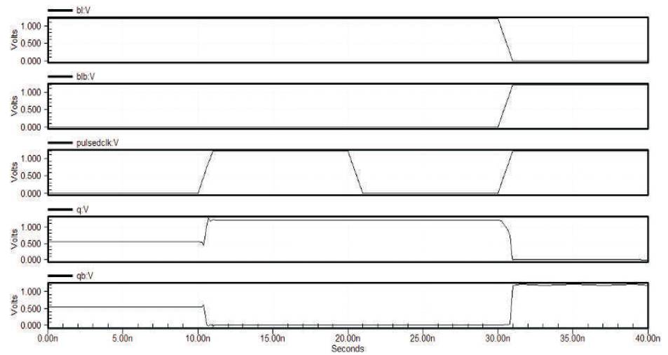
Figure 5( c). Waveform of 1bit SRAM Cell using Pulsed Latch in 90 nm Technology
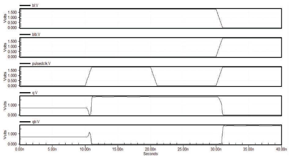
Figure 5(d). Waveform of 1bit SRAM Cell using Pulsed Latch in 180 nm Technology
The 8 bit SRAM cell consist of eight 1bit sram cell, and each cell has its own input and output lines, also each cell is connected to a common pulsedclk signal. A pulsedclk signal is just like a wordline signal in a simple SRAM cell. The cell consist of data input ' bl' and complementary data input 'blb' with a pulsedclk signal, also it consists of data output 'q' and complementary data output 'qb'. The schematic of 8 bit SRAM cell is shown in Figure 6(a).
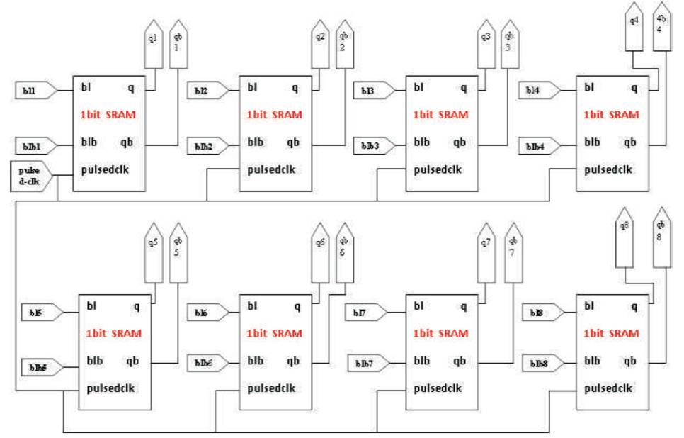
Figure 6 (a). Schematic of 8 bit SRAM Cell using Pulsed Latch
The waveform of 8bit SRAM cell using pulsed latch in three different technologies that is 45 nm, 90 nm and 180 nm CMOS technologies are shown in Figure 6(b), 6(c) and 6(d). The schematic diagram of 8 bit SRAM cell using pulsed latch circuit, which is shown in Figure 6(a) is in 45 nm technology.
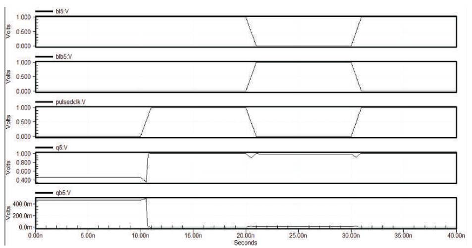
Figure 6 (b). Waveform of 8 bit SRAM using Pulsed Latch in 45 nm Technology
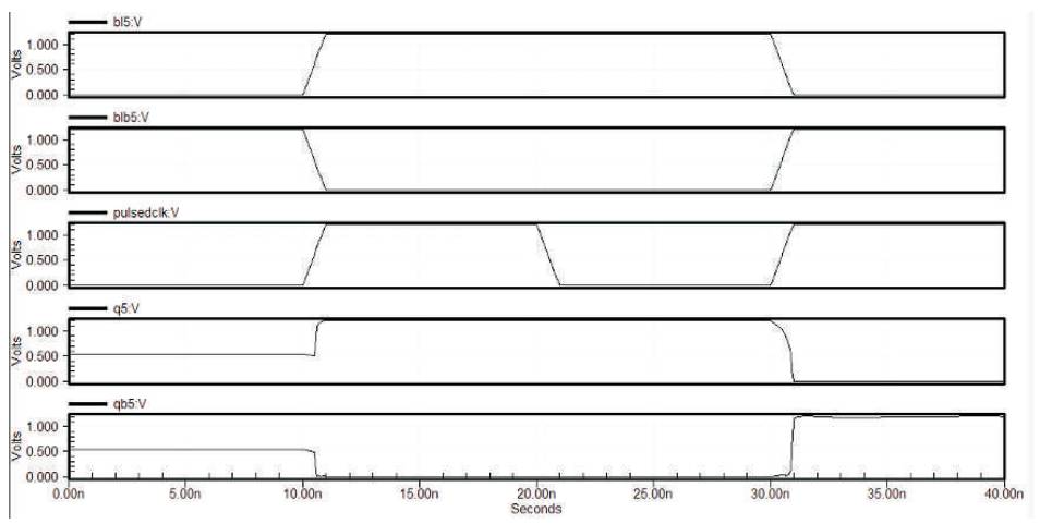
Figure 6 ( c). Waveform of 8 bit SRAM Cell using Pulsed Latch in 90 nm Technology
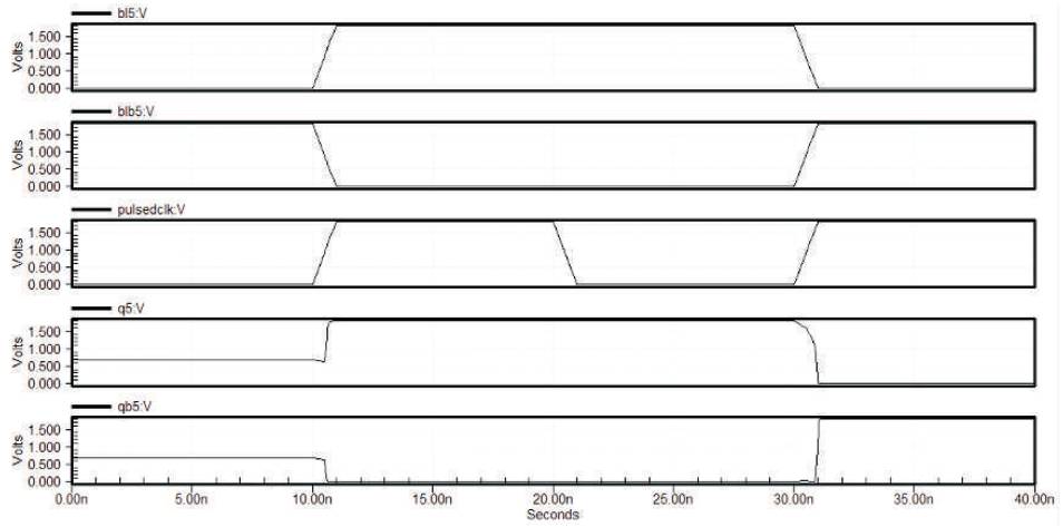
Figure 6 (d). Waveform of 8 bit SRAM Cell using Pulsed Latch in 180 nm Technology
In this section, the power and delay of 1bit and 8 bit SRAM cell is compared. The comparision has been done between conventional SRAM cell and the proposed SRAM cell. The authors have designed SRAM cell in three different CMOS technologies. In the above sections, it is clear that the waveforms are same for both 1bit and 8 bit SRAM cell in the proposed and conventional SRAM cell design. They have designed SRAM cell in different technologies with different supply voltage. In 45 nm technology supply voltage is 1V whereas for 90 nm and 180 nm technology, the supply voltage is 1.2V and 1.8V respectively.
From the above simulation results it is clear that the delay and power of the proposed SRAM cell is lower than that of the conventional SRAM cell.
In the previous sections, the authors have compared the design of SRAM cell between conventional SRAM cell and proposed SRAM cell for 1 bit and 8 bit cells in different CMOS technologies. The results obtained are shown in Tables 1-6. So, from the obtained results, it can be concluded that the proposed method works better than the conventional SRAM cell design. The main aim of this design approach is to reduce delay so as to increase the speed of the SRAM cell. The proposed methodology can be applied to n number of bits which results in low power and delay.
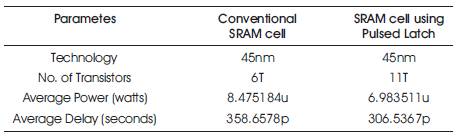
Table 1. Simulation Result of 1 bit SRAM Cell in 45 nm Technology
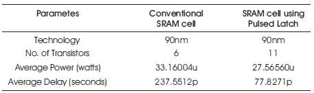
Table 2. Simulation Results of 1 bit SRAM Cell in 90 nm Technology
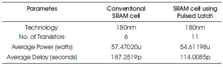
Table 3. Simulation Results of 1 bit SRAM Cell in 180 nm Technology
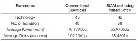
Table 4. Simulation Results of 8 bit SRAM Cell in 45 nm Technology
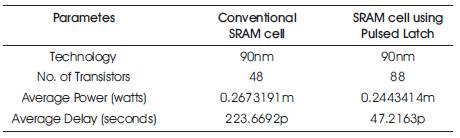
Table 5. Simulation Results of 8 bit SRAM Cell in 90 nm Technology
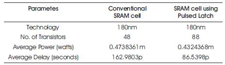
Table 6. Simulation Results of 8 bit SRAM Cell in 180 nm Technology
The gratitude we feel for the immense support of the number of people for the completion of my research work cannot be expressed in mere words. I take this opportunity to acknowledge my gratitude towards Assistant Professor Khemraj Deshmukh for providing excellent guidance and inspiration throughout my research work. We would also like to thank all the respected faculty members at SSGI, Bhilai for giving their valuable time and guidance, for the completion of this work.