(1)
In digital VLSI, sequential elements are most power consuming components. Flip-Flops are the basic storage elements and subsystem of clock distribution network which consume large amount of power. Nowadays for digital design, designers use pipelining techniques to design flip-flop based systems, such as shift registers and register files. In this paper, Pulse Triggered Flip-flop (P-FF) is discussed and Serial in Serial out (SISO) shift register is designed as its application. The main objective of this paper is to optimize the area and power of the shift register for use in Application Specific Integrated Circuits (ASICs) and embedded systems. This paper demonstrates the design of SISO shift registers in three different ways. First shift register is simple in structure and designed only by using P-FF. Second shift register uses clock gating circuit to reduce the switching power consumption and third design of shift register, pulse generator of P-FF is shared among all the latches. These three different SISO shift registers are compared in terms of power dissipation and transistor counts. Shift register has been designed at schematic level and simulated using Tanner EDA at CMOS 32nm BSIM4 technology. The simulation results of SISO shift register with common pulse generator shows effective reduction of power consumption and transistor count.
With increase in clock frequency and transistor count, power dissipation of digital CMOS design has increased and now for a VLSI designer, power conservation is a primary constraint. In past power dissipation was not a primary constraint because operating frequency and chip capacity were low. Nowadays as scale of integration improves, high performance battery based devices are being developed so designs that consumes low power while maintaining comparable performances are needed [8].
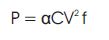
The CMOS digital circuit's power dissipation is two types: (1) Static power dissipation and (2) Dynamic power Dissipation. Static power dissipation is mainly due to leakage current. Dynamic power dissipation can be divided in two types: Short circuit power and switching power.
The equation used to calculate the power dissipation in CMOS circuit is given by,
where α is the data switching activity, C is the capacitance, f is the frequency, and V is the supply voltage.
Switching power is more dominant in CMOS circuit [2], [4]. This paper concentrates to reduce the switching power by avoiding unnecessary switching activities.
Shift register consists of flip-flops and to design a low power shift register, power consumption in a flip-flop must be reduced.
In synchronous VLSI, flip-flops consume large amount of power because these subsystems are clocked with system operating frequency. For low power VLSI system, careful design of latches and flip-flops are important [3], [7].
In high performance microprocessors, in order to reduce total chip power, reduction of clock power is an important approach [1], [12]. To conserve power in a shift Register, unnecessary switching activity at internal nodes must be avoided when input patterns remains unchanged.
This paper is organized as follows. Section 1 gives brief knowledge of Clock gating technique which will be later used to minimize the switching power of SISO shift register. Section 2 presents pulse triggered flip-flop which is an existing design. Section 3 shows different designs of SISO shift register. Section 4 shows simulation results and the last section concludes this work.
Figure 1 shows the concept of traditional XOR based clock gating scheme and Figure 2 shows the waveform of gated flip-flop. Clock gating is an important technique to reduce the dynamic power dissipation by blocking the clock signal. During the idle cycles of flip-flop, clock gating technique cuts off the clock [9], [14], [15].
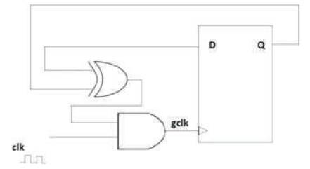
Figure 1. Concept of Clock Gating
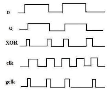
Figure 2. Waveform of Gated Flip-Flop
The operation of gating scheme is as follows:
A Pulse Triggered Flip–Flop (P-FF) consists of a pulse generator and a latch. Pulse generator is for strobe signals and a latch for data storage. The latch act as an edge triggered flip-flop if the triggering pulses are sufficiently narrow. Due to its single-latch structure and for high speed application, Pulse-triggered flip-flop is more popular than the conventional transmission gate and master-slave based flip-flop [5].
Figure 3 shows schematic of Pulse triggered flip flop. This flip-flop is a high speed option in wide-operating-range cell library [6]. Figure 3(a) shows schematic of pulse generator. Clock is applied to pulse generator circuit.
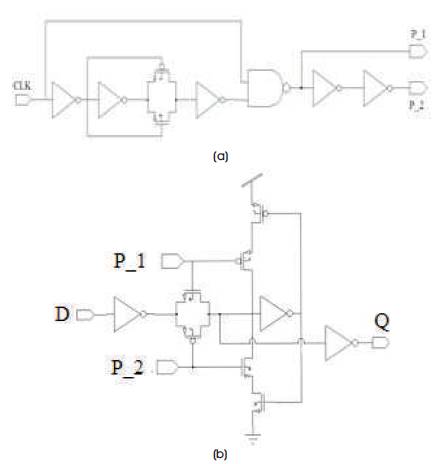
Figure 3. Pulse Triggered Flip-Flop (a) Pulse Generator (b) Pulsed Latch
This Pulse generator circuit produces two pulses P_1 and P_2 for every rising edge of the clock. These pulses are opposite to each other. P_1 is a positive pulse, while P_2 is a negative pulse. The inverter chain produces phase difference and delay. The effective width of pulses depends on the delay of inverters. Here three inverters are used, 5 inverters or 7 inverters can be also used to generate delay. 3 inverter delay cannot generate valid pulse for voltage below 0.7 [6].
Figure 3(b) shows schematic of latch. This flip-flop performs operation only when it receives positive pulse at node P_1 and negative pulse at node P_2. Low power keeper structure and low latency path is the advantage of this flip-flop.
Figure 4 shows the waveform of pulse generator. Whenever CLK goes from 0 to 1, it generates positive and negative pulses. In pulse triggered flip-flop, pulse generator can be classified in two types: an implicit or an explicit type. In an implicit type, the pulse generator is part of the latch design and no explicit pulse signals are generated. In an explicit type, the pulse generator and the latch are separate [13].
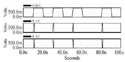
Figure 4. Waveform of Pulse Generator
Here explicit type pulse generator is used. The disadvantages of explicit type pulse generator is, it consumes more power than implicit type. But explicit type pulse generator provides a high speed operation.
Shift registers are a group of flip-flops mainly used for storage of digital data. The output of one flip-flop is input to the next flip-flop, which results in shifting of bits. In SISO shift register, the input data is applied serially, i.e. one bit at a time on a single line and produces the stored information on its output also in serial form. Figure 5 shows four bit SISO. In this SISO, each block consists of pulse triggered flip-flop. The internal structure of P-FF is pulse generator and latch. Clock signal is applied to the pulse generator of each P-FF. Pulse generator generates two small pulses which is applied to latch.
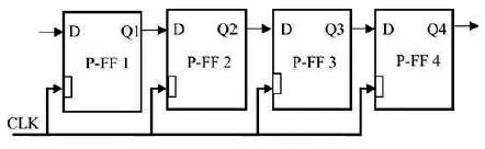
Figure 5. Four Bit SISO Shift Register
Figure 6 shows four bit SISO with clock gating scheme. To reduce the power of above four bit SISO, clock gating technique is adopted. Switching power dissipation is more dominant in sequential circuit, clock gating technique avoids unnecessary switching in this shift register.
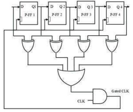
Figure 6. Four Bit SISO Shift Register with Clock Gating
The input and output of each P-FF is applied to X-OR gate and the output of X-OR will set only when input and output of P-FF is different. All the output of XOR gate is given to OR gate and output of OR gate is applied to AND gate.
Clock is applied through the second input of AND gate. When clock is zero, then gated clock will be also zero and When clock is one, then gated clock depends on the output of OR gate.
Figure 7 shows SISO Shift Register with common pulse generator. Clock is applied to the pulse generator and this pulse generator produces two pulses P_1 and P_2 for every rising edge of clock. These pulses are shared by all the four latches. Here explicit pulse generator are used to generate the pulses. The advantage of explicit pulse generator is to provide high speed and the disadvantage is it has a high power dissipation. By sharing the pulse generator, power can be minimized as well as the area.
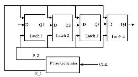
Figure 7. Four Bit SISO Shift Register with Common Pulse Generator
The simulation results are carried out using Tanner EDA by using BSIM4 32nm technology file at room temperature. The circuit is simulated at schematic level and supply voltage VDD is maintain at 0.9 V.
Figure 8 shows the simulation result of four bit shift register. The average power consumed by this design is 10 μw.
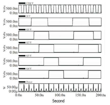
Figure 8. Simulation Result of Four Bit SISO Shift Register
Figure 9 shows the simulation result of four bit SISO shift register with clock gating scheme. This design consumes 5.5 μw power, which is 45% less from SISO shift register without clock gating.
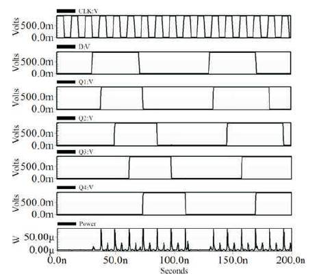
Figure 9. Simulation Result of Four Bit SISO Shift Register with Clock Gating
Figure 10 shows the simulation result of four bit SISO with common pulse generator. This design is efficient in terms of area and power. The power consumed by this design is 3 μw, which is 70% low from first design and 45% low from second design.
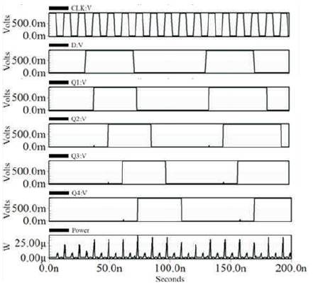
Figure 10. Simulation Result of SISO Shift Register with Common Pulse Generator
The comparison of different SISO shift registers is shown in Table 1. From this table, it is clear that four bit SISO shift register with common pulse generator consumes less power and is also efficient in terms of area.
Table 1. Comparison of Shift Registers in terms of Power and Transistor Count
In this paper, three types of P-FF based shift register designs are discussed. These shift registers are simulated in Tanner EDA by using CMOS 32nm BSIM4 technology file. Shift Register with clock gating consumes less power, but not efficient in term of area. The comparison and simulation results show, shift register with common pulse generator is more efficient in terms of both power and area.
The authors would like to thank the management, SSTC SSGI institute for providing Tanner EDA Tool v15.0.