(1)
A new realization of Differential Voltage Current Conveyor (DVCC) is presented in this paper. It uses CMOS inverters operating in transconductance mode of operation. The port relationships have been analytically modelled and are verified through SPICE simulations using TSMC 0.18 μm CMOS process parameters. Larger bandwidth, ability to operate at lower supply voltage and synthesis using digital CMOS inverters are the key advantages of the proposed realization over the traditional DVCC. The usability of the proposed DVCC is illustrated through an application.
The CMOS inverter is an integral part of digital circuits and is widely used in applications ranging from simple as latches to the complex ones like multipliers and processors. The simplicity and ease with which the CMOS inverter is being used in digital domain has motivated researchers to use it for analog circuits. It is well known that a CMOS inverter can be used as transconductance amplifier [1, 2] . Automatic synthesis on silicon with the help of digital tools is another impetus for inverter based analog building block realization [3, 4]. Thus, the objective of this paper is to introduce a new topology of Differential Voltage Current Conveyor (DVCC) based on CMOS inverters only. The proposed topology has some significant advantages over the traditional topology.
This paper is organized as follows. Section 1 presents a brief overview of traditional DVCC, followed by operation of the CMOS inverter as a transconductance element in section 2. An inverter based realization of DVCC is proposed in section 3 and its port relationships are analytically modeled. In Section 4, the functional verification of the proposed topology is carried out using SPICE and its performance is compared with traditional DVCC. Post layout simulation results are also included for the sake of completeness. A Multi Input Single Output (MISO) second order filter using proposed DVCC structure is realized as an application in section 5 which is followed by conclusion in the last section.
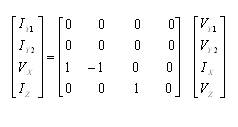
The DVCC is a variant of current conveyor and is useful for differential and floating input signal processing circuits [5- 9] . The circuit symbol of DVCC is shown in Figure 1 and its port relationship is characterized by equation (1).
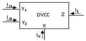
Figure 1. Circuit Symbol of DVCC
The CMOS based realization of DVCC is shown in Figure 2 [5, 6]. It has two high input impedance terminals (Y , Y ) 1 2 which can be used for differential voltage sensing and the difference is available at low impedance X port. This action is done by the differential pairs M - M and M - M . 1 2 3 4 The current at X port is conveyed to high impedance Z terminal with the help of transistors M - M .
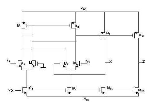
Figure 2. CMOS Realization of DVCC [5, 6]
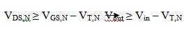
The CMOS inverter is shown in Figure 3 which is designed using an NMOS (M ) and a PMOS (M ) transistor with their N P aspect ratios denoted as W /L and W /L , respectively. N N P P Figure 4 shows DC Voltage Transfer Characteristics (VTC) curve of CMOS inverter. The VTC of inverter has steepest slope around switching threshold voltage (V ) which is th defined as the voltage at which V = V . At this voltage, out in both the transistors operate in saturation region [2]. The condition for saturation region operation of transistors M N and M are given respectively as,
and

where V and V are threshold voltages of M and M , respectively.
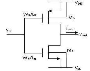
Figure 3. Traditional CMOS Inverter Transistor Configuration
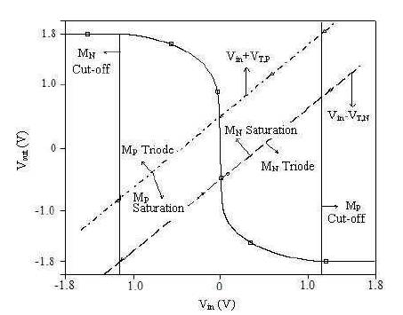
Figure 4. DC Characteristics of CMOS Inverter (for V = -V = 1.8 V)
Further the voltage V falls exactly in the middle of the VTC th for a symmetric inverter, wherein the aspect ratios for NMOS (W / L ) and PMOS(W / L ) are related by W = (μ /μ ) N N P P P N P W for L =L [10]. The value of V for such an inverter will be N N P th zero if power supplies are chosen as V = -V .
The small signal model of CMOS inverter is shown in Figure 5, wherein V and V denotes small signal input and in out output voltages, respectively. The small signal output current (i ) of inverter is given by i = -g V , where g is out out m in m transconductance of inverter around switching threshold which is given by g = (g + g ), g and g , respectively m mN mP mN mP representing transconductances of transistors M and M . N P Thus the CMOS inverter behaves as a transconductor for small signal amplitudes about V . The CMOS inverter I-V th characteristic in transconductance mode of operation is shown in Figure 6.
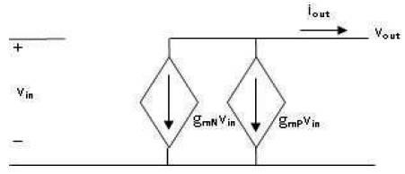
Figure 5. Small Signal Equivalent of CMOS Inverter when both Transistors MN and MP are in Saturation
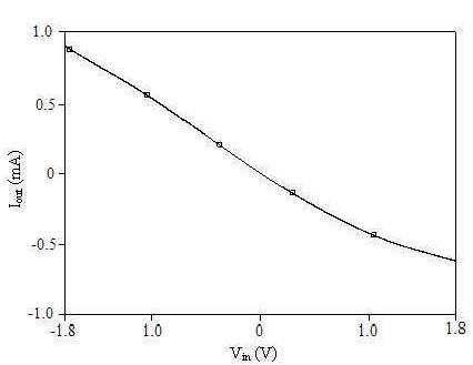
Figure 6. I-V Characteristics of CMOS Inverter when Input is Shorted to Output
The proposed DVCC circuit is constructed using CMOS inverters and is shown in Figure 7. The aspect ratios of NMOS and PMOS of CMOS inverter are set such that the switching threshold of the inverter is obtained at (V SS +V )/2. In order to establish the port relationships, the DD small signal model of the proposed DVCC is drawn as shown in Figure 8. The output conductances of the transistors are neglected to simplify the analysis. Here, g mi th represents the transconductance of i inverter for i = 1 to 10. The resistances R and R are loading resistances at LX LZ node X and Z, respectively, and the capacitances C , C , N X and C represent parasitic capacitances at nodes N, X, Z and Z, respectively. It may be noted that the proposed structure has only one intermediate node 'N' and the resistance R at node N is equal to as the inverters 3 N and 4 have their respective input and output terminals shorted.
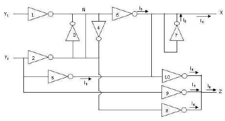
Figure 7. Proposed DVCC based on CMOS Inverters
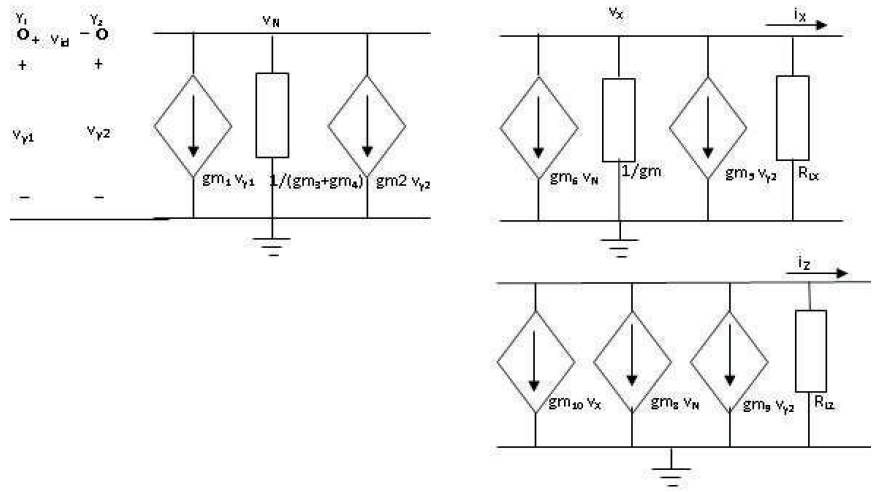
Figure 8. Small Signal Model of Proposed DVCC
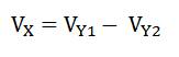
The relationship between voltages of Y , Y , and X ports (V , 1 2 Y1 V and V , respectively) can be established by observing Y2 X the section of Figure 7 comprising of inverters 1 to 7. By using routine analysis, ignoring the effect of parasitic capacitances at node N, X, and Z, the dependence of V X on V and V is computed as:
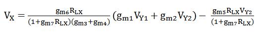
Considering g = g = g = g = g = g (say), and g m1 m2 m3 m4 m7 m m5 = g = 2g , equation (4) simplifies to,
where R = 1/g . X m
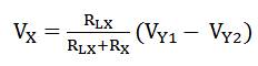
If R R , then equation (5) can be rewritten as,
This confirms the relationship between Y1, Y2, and X ports of the proposed DVCC.
Taking the parasitic capacitances at node N, X, and Z into account, the voltage transfer function (4) modifies to,
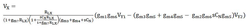
The assumptions g = g = g = g = g = g ; g = m1 m2 m3 m4 m7 m m5 g = 2g simplify equation (7) to,
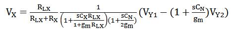
It may be noted from equation (9) that the performance of DVCC deviates from the ideal one at higher frequencies. Equation (9) reduces to the ideal port relationship given by equation (6), if operating frequencies are chosen much lower than min ( ).
It may be observed from Figure 7 that, the current transfer from X to Z port is represented by inverters 5 to 10. The sum of currents flowing out of inverters 5-7 (I , I , I ) is designated 1 2 3 as the current through X port (I ) and that through inverters X 8-10 (I , I , I ) represents Z port current (I ). The selection g 4 5 6 Z m9 = g , g = g , g = g results in I = I , I = I , and I = I , m5 m8 m6 m10 m7 4 3 5 1 6 2 thereby making I = I which implies that the current of Z Z X port follows the X port current.
Taking the parasitic capacitances into account, the current transfer function from X to Z port, is computed as,
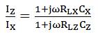
However by choosing frequency sufficiently below min(1/(R G ), 1/(R G )), the effect of parasites can be ignored.
The functionality of the proposed DVCC is verified through SPICE simulations using TSMC model parameters of 0.18 μm CMOS process. The supply voltage of V = -V = 1.8 V DD SS are used. The aspect ratios of CMOS inverters are given in Table 1.
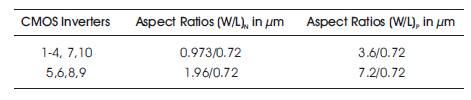
Table 1. CMOS Inverters’ Aspect Ratios for Proposed DVCC in Figure 7
The theoretical and simulated voltage and current transfer characteristics of the proposed DVCC are shown in Figures 9 (a) and (b), respectively. It is clear that the voltage at X port tracks the voltage difference between Y 1 and Y ports in the range of -400 mV to +400 mV and Z port 2 follows the X port current variation between -300 to 300μA. The magnitude response of voltage and current transfers, input and output noise spectral densities, and total harmonic distortion are shown in Figure 10. The voltage transfer function is plotted by exciting proposed DVCC with a differential input of 0.5 V while keeping output port open-circuited. The current transfer is observed by applying an input current of 100 μA and keeping Z port short-circuited. The voltage and current transfer bandwidths are found to be 843.3 MHz and 1467.3 MHz, respectively. The proposed DVCC is also simulated for lower values of power supply V = -V = 0.5 V. The DC DD SS characteristics are shown in Figure 11 which conforms to the functionality. Thus the structure can operate at low supply voltage also.
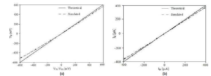
Figure 9. DC Transfer Characteristics of Proposed DVCC for V = -V = 1.8V (a) V vs. (V -V ) Curve, (b) I vs. I Curve
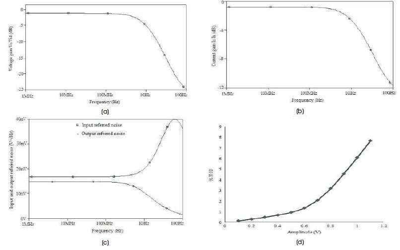
Figure 10 (a) Frequency Response of Voltage Transfer Function, (b) Frequency Response of Current Transfer Function, ( c) Input and Output Voltage Referred Noise Spectral Densities, (d) X port THD for 3 MHz Input Frequency
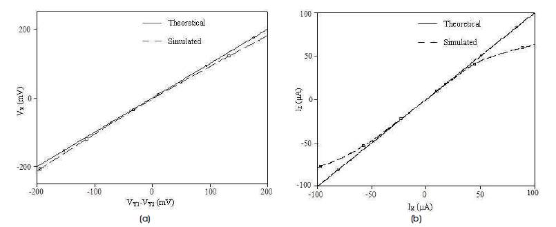
Figure 11. DC Transfer Characteristics of Proposed DVCC for V = -V = 0.5 (a) V vs. (V -V ) Curve, (b) I vs I Curve
To draw a fair comparison, the traditional DVCC was also simulated, for power supply values of ± of 1.8 V and ±0.5V while VB values were chosen to be -1.1 V and -0.1 V, respectively using TSMC 0.18 μm CMOS process parameters. The aspect ratios using all transistors are given in Table 2. Various performance parameters of the traditional and proposed DVCC are recorded for both the sets of power supply values in Table 3 and it is observed that the proposed DVCC outperforms in most of the performance parameters.
Table 2. Transistor Aspect Ratios for Traditional DVCC in Figure 2
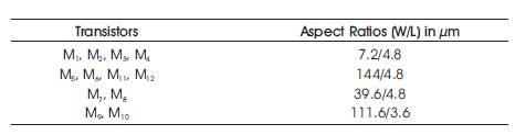
Table 3. Simulated Characteristics of the Proposed and Traditional DVCC
The proposed DVCC circuit is also laid-out using Microwind 3 VLSI CAD tool with optimized sizing and spacing in conformity to the design rules of 0.18 μm CMOS process. The layout is shown in Figure 12.
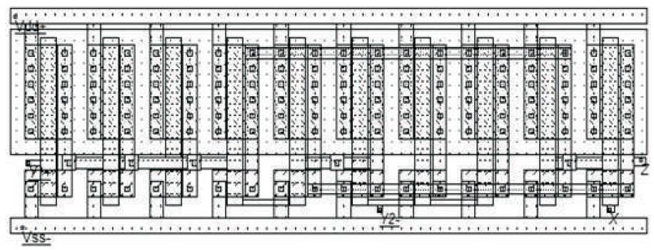
Figure 12. Layout Overview of Proposed DVCC
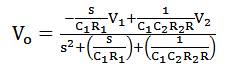
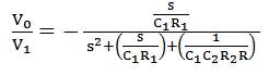
In this section, the proposed DVCC is used to implement a MISO second-order filter (Figure 13) [8]. Lowpass and bandpass responses are achieved depending on the active input. The output voltage of the filter configuration of Figure 13 is given by,
By activating input V and making V = 0, equation (11) modifies to a bandpass response as,
Similarly, for V = 0 and V as an active input, equation (11) 1 2 changes to a low pass response,
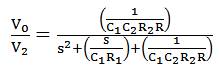
The parameters w and Q of the MISO filter are given by,
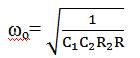
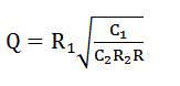
The circuit of Figure 13 uses resistances R and R 2 connected at X port, which can be realized with the internal resistance (1.83 KΩ) of the proposed DVCC. The filter is simulated with R = 1.83 KΩ and C = C = 100 pF, 1 1 2 and the results are shown in Figure 14. The cutoff frequency is approximately 860 KHz, which is in close agreement to the theoretically calculated value of 869 KHz.
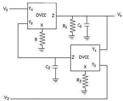
Figure 13. Circuit Realization of MISO Filter
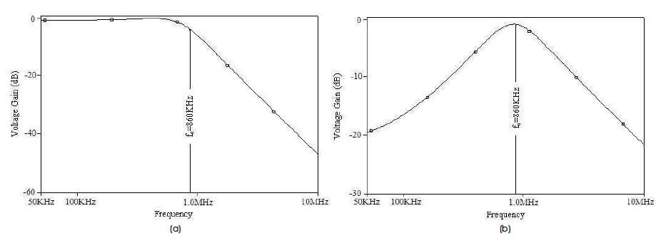
Figure 14. Simulated Frequency Response of MISO Filter (a) Lowpass, (b) Bandpass
A new CMOS inverter based realization of differential voltage current conveyor is introduced in this paper. Analytical modeling of port relationships have been presented and are verified through SPICE simulations using TSMC 0.18 μm CMOS process parameters.
The proposed DVCC circuit is also laid-out using Microwind 3 VLSI CAD tool. A comparison between proposed and traditional DVCC is also drawn in terms of various performance parameters. Larger bandwidth, better noise performance, and ability to operate at lower supply voltage are the key advantages of the proposed realization over the traditional DVCC. A MISO filter structure using proposed DVCC is also presented as an application and various results are found in conformity with the theoretical propositions.